

설명
설명 없음환경 설정
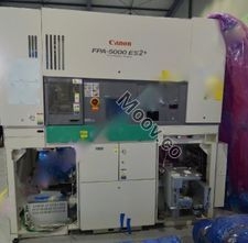
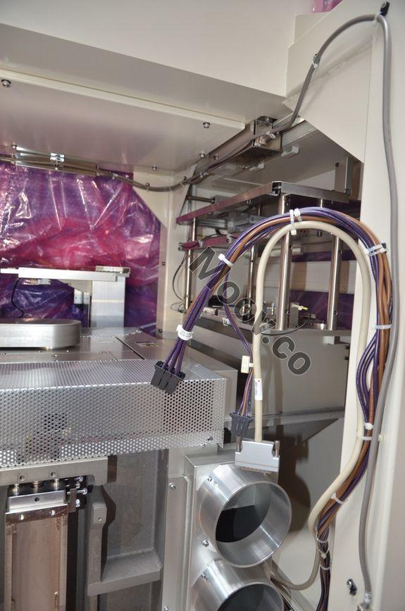
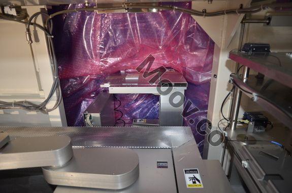
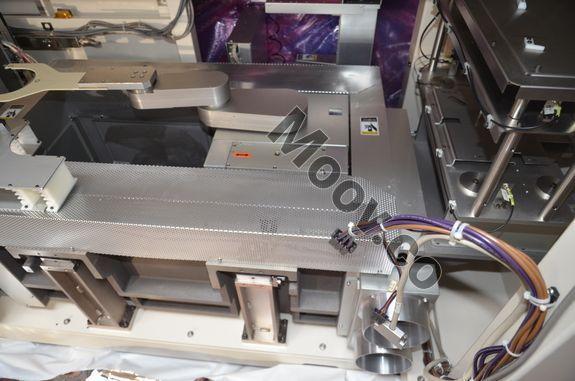
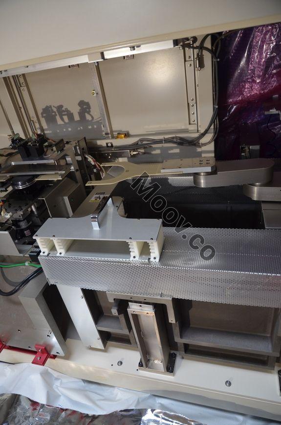
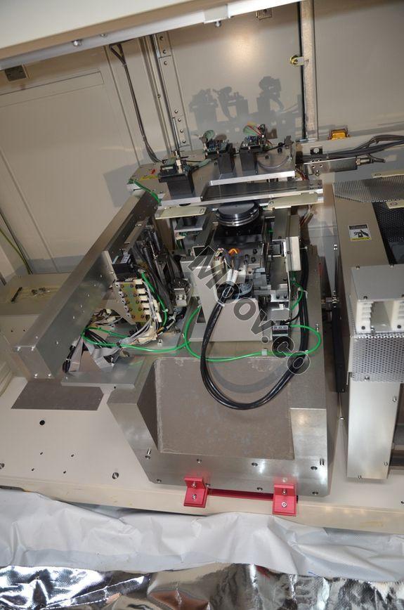
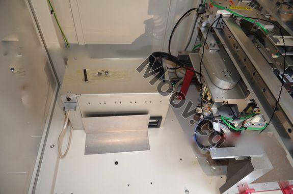
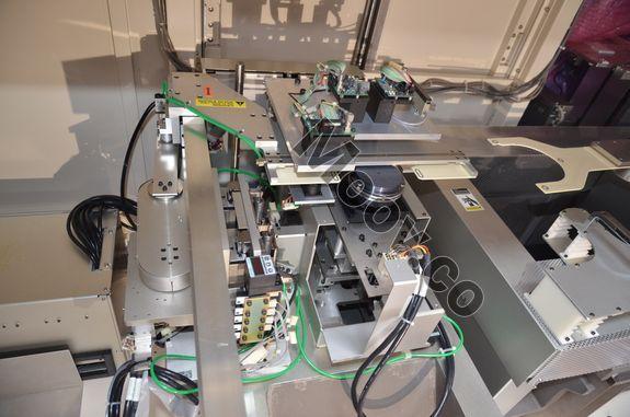
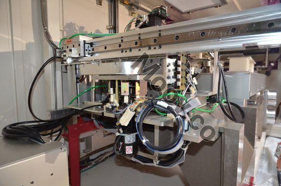
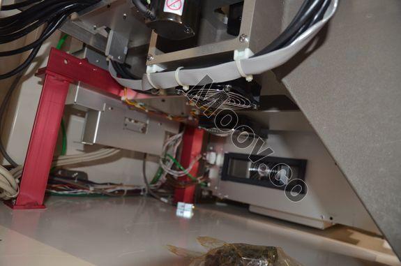
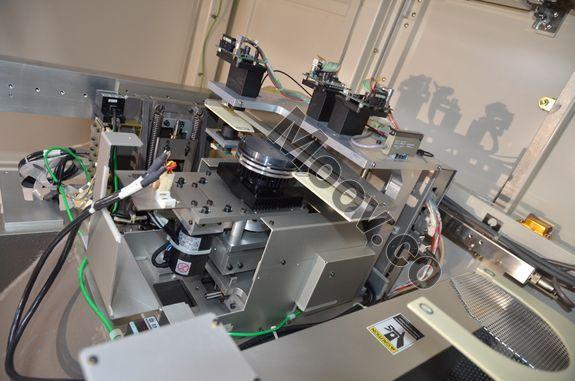
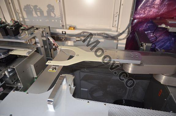
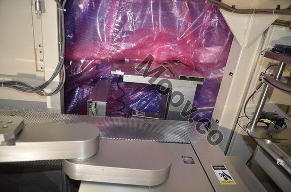
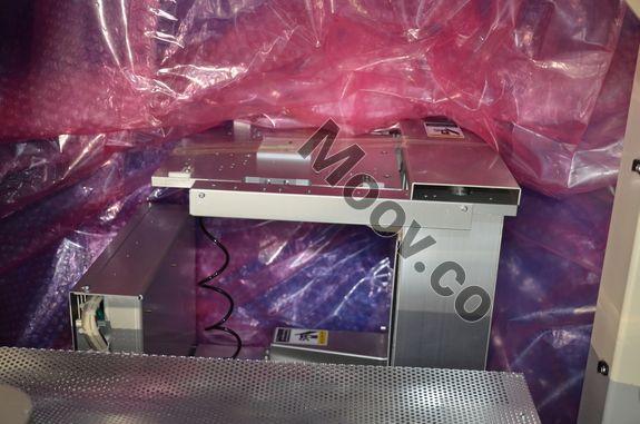
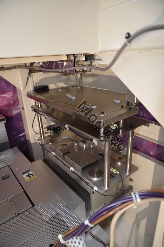
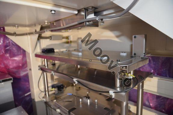
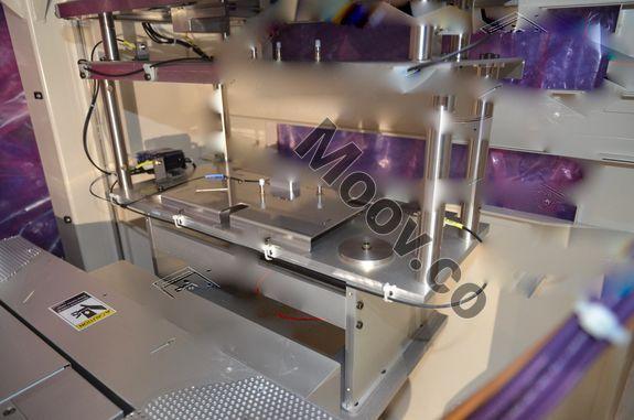
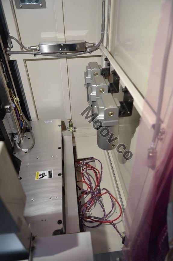
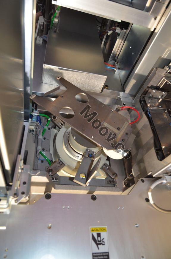
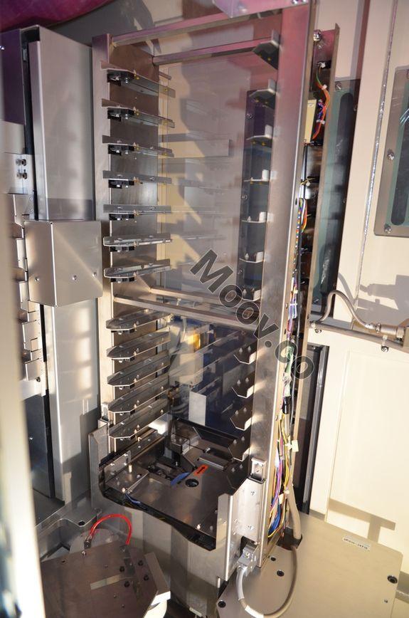
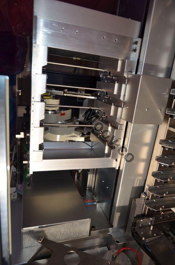
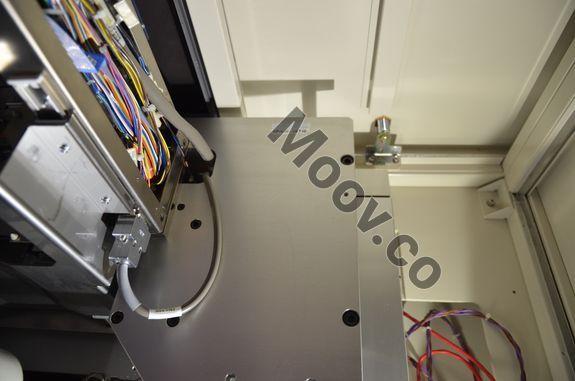
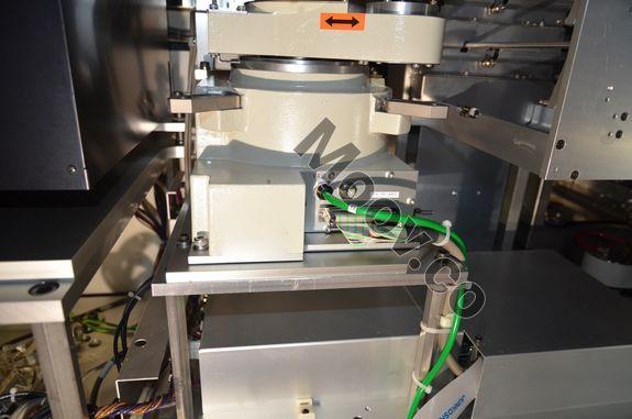
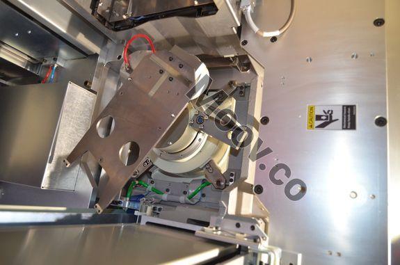
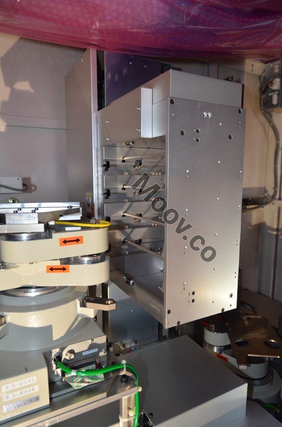
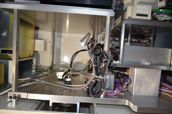
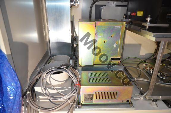
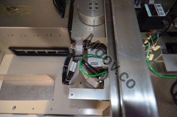
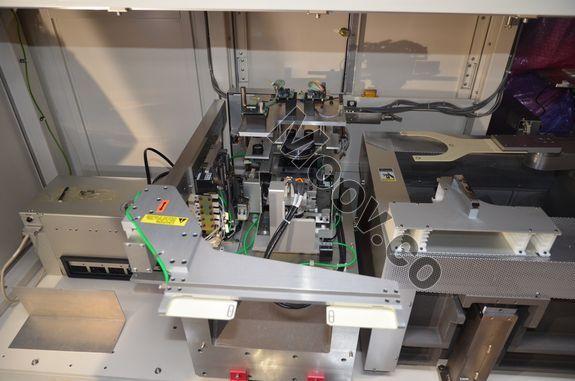
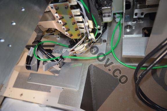
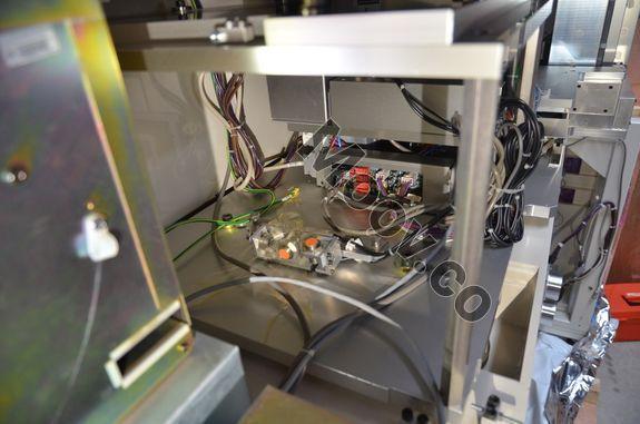
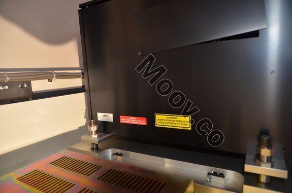
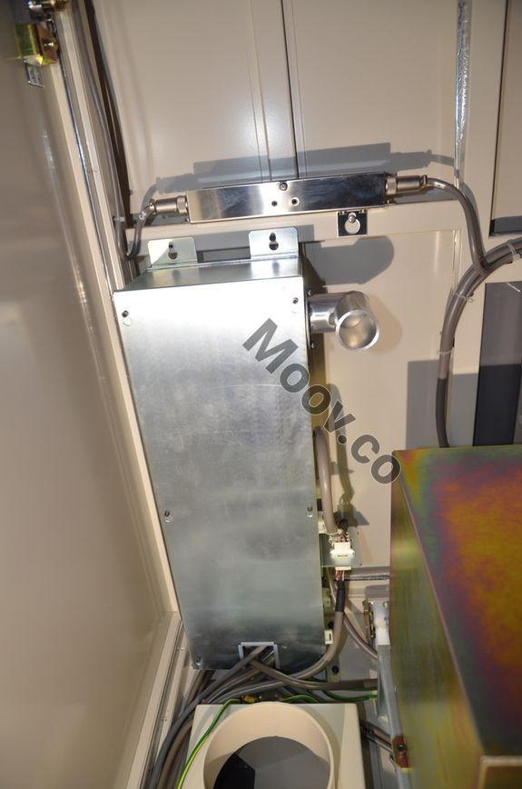
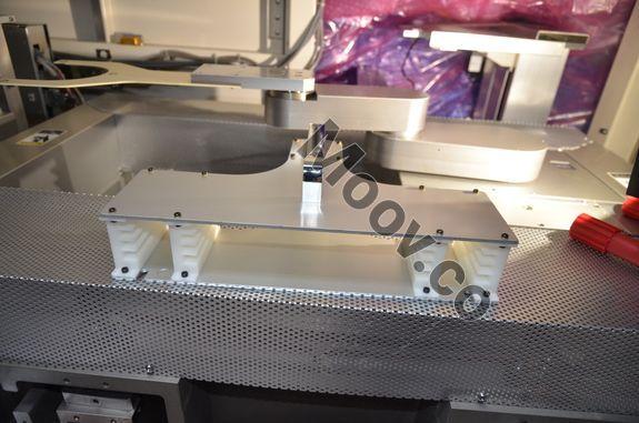
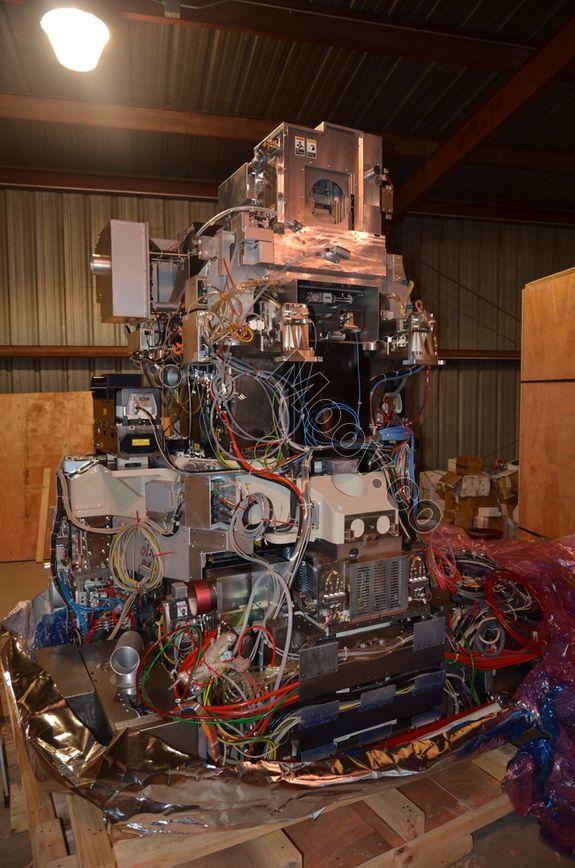
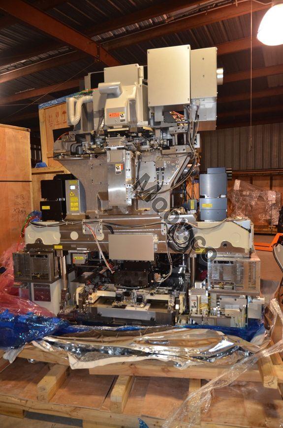
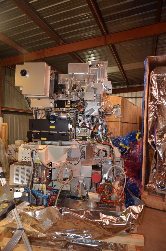
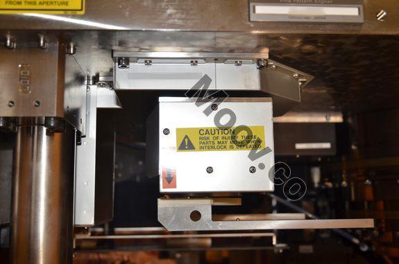
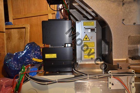
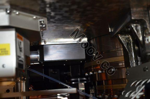
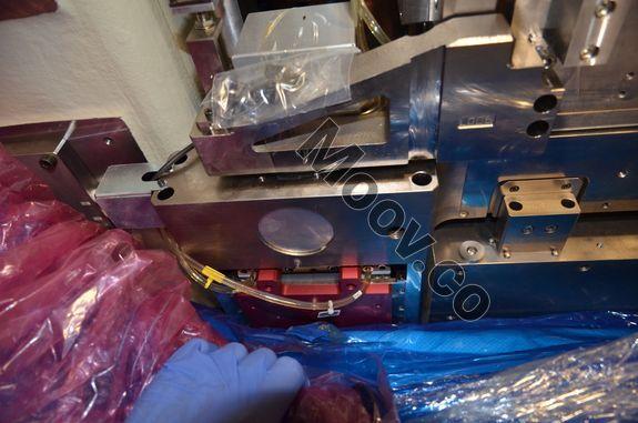
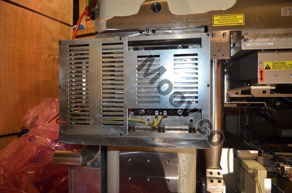
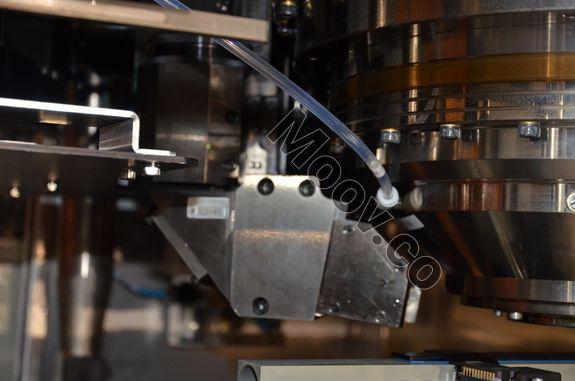
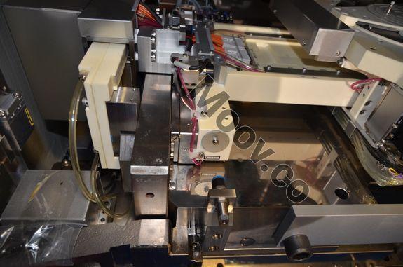
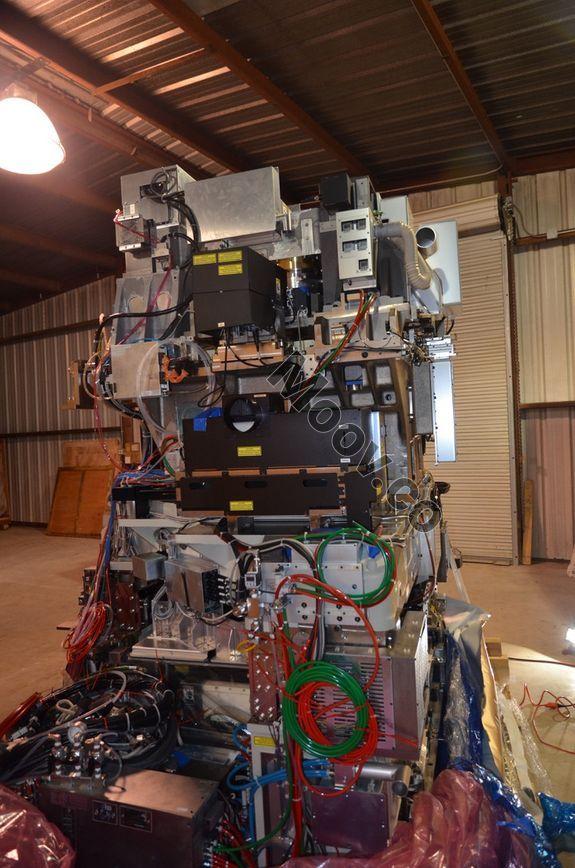
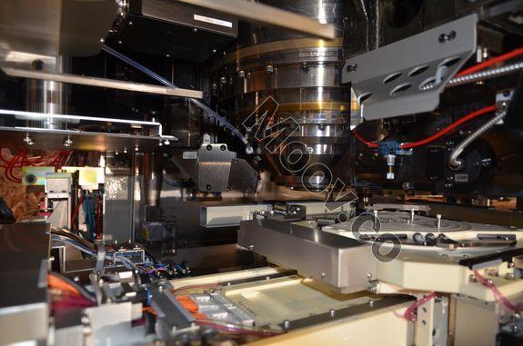
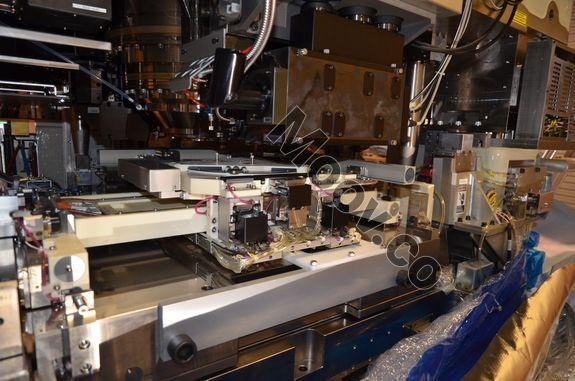
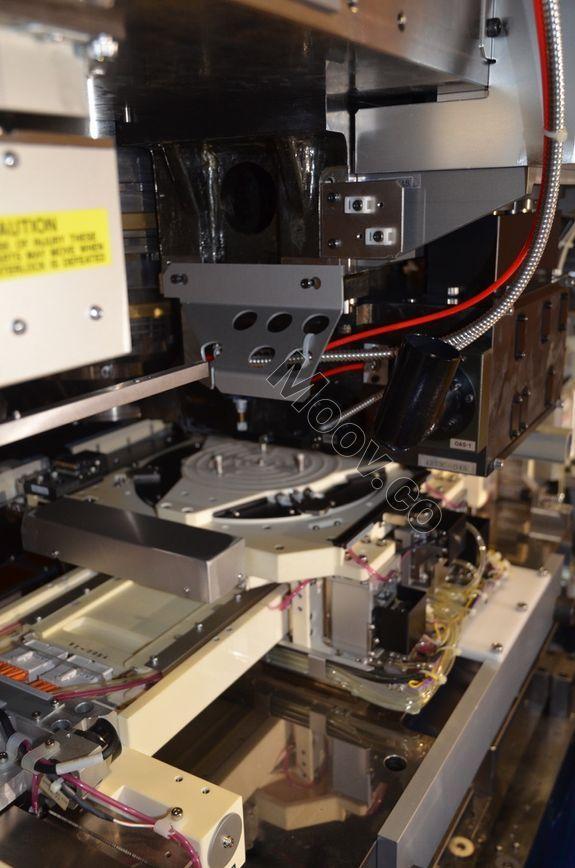
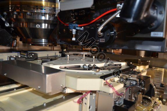
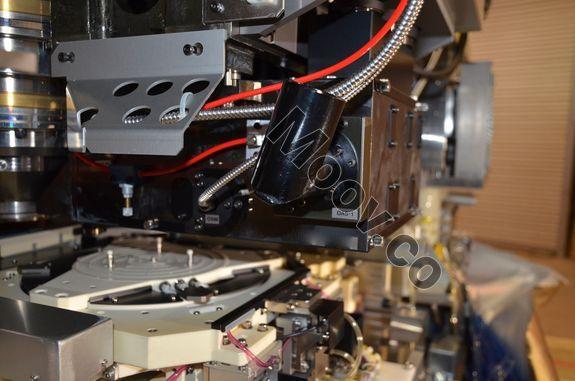
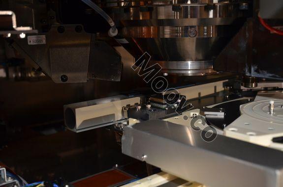
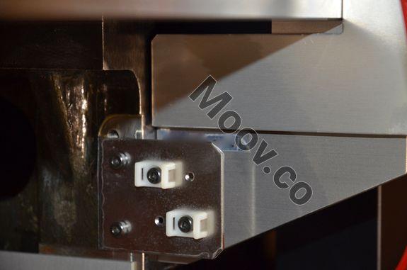
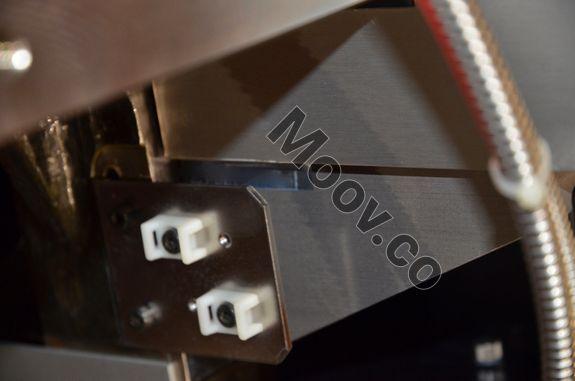
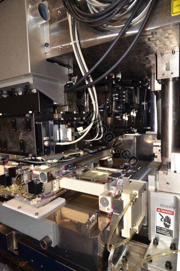
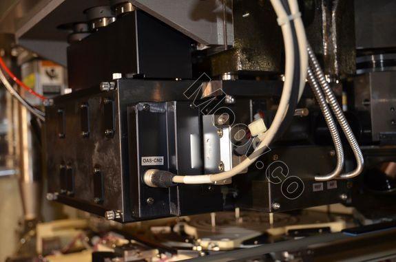
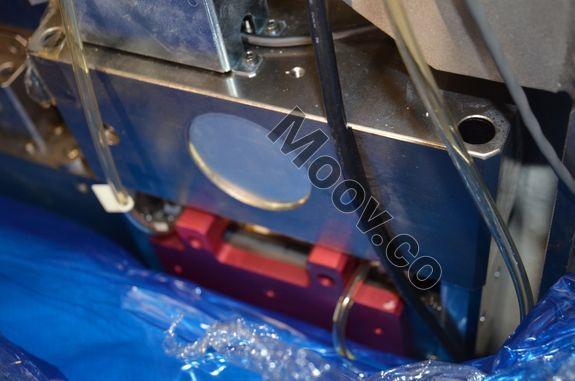
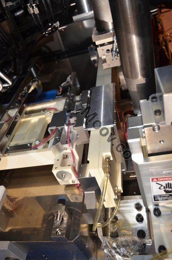
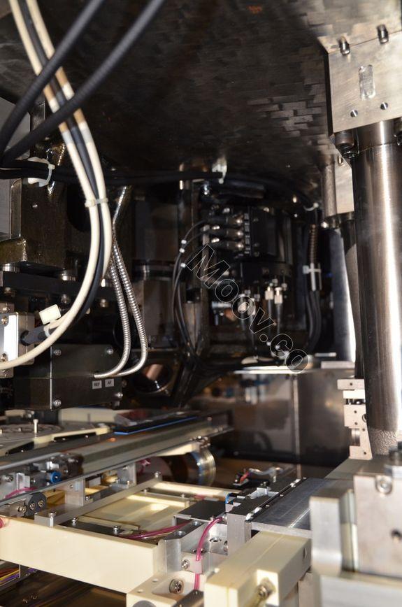
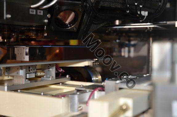
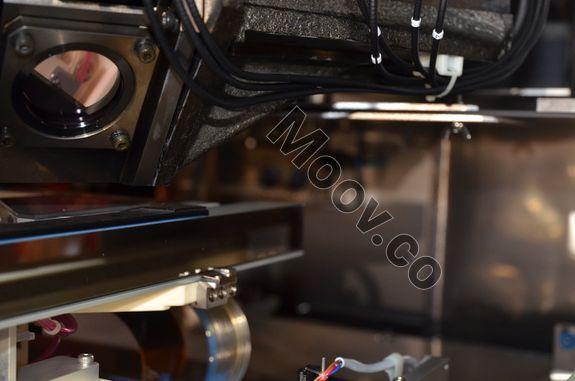
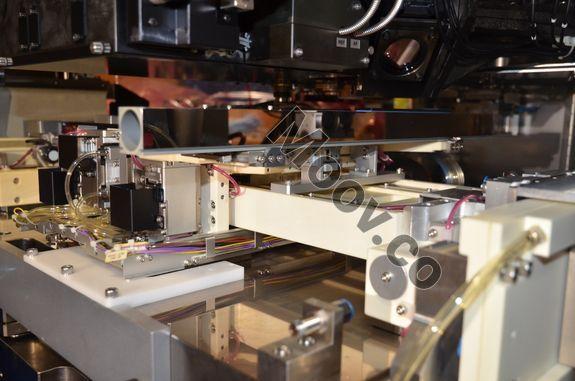
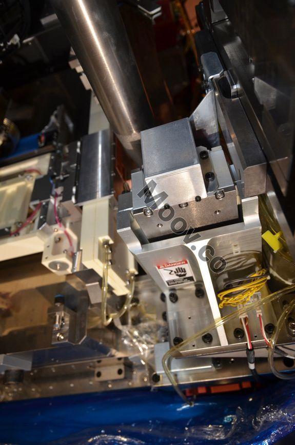
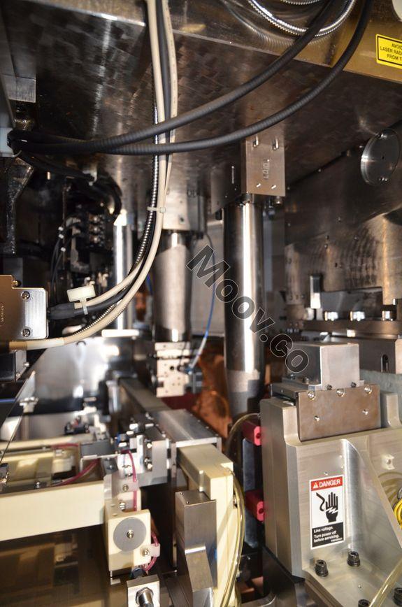
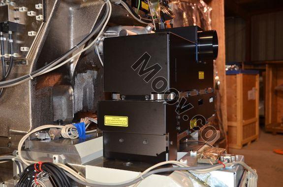
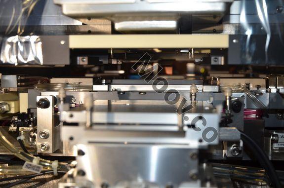
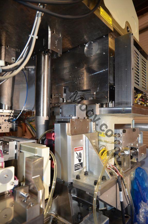
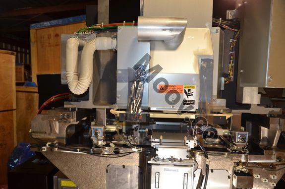
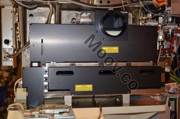
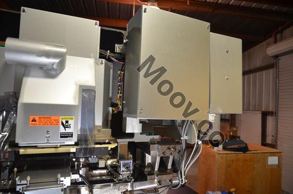
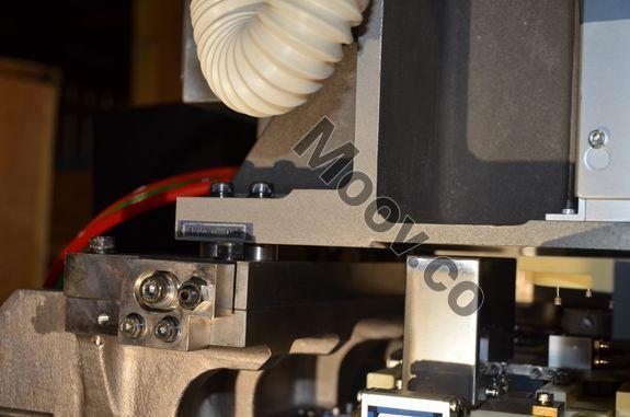
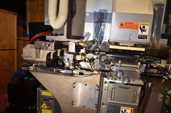
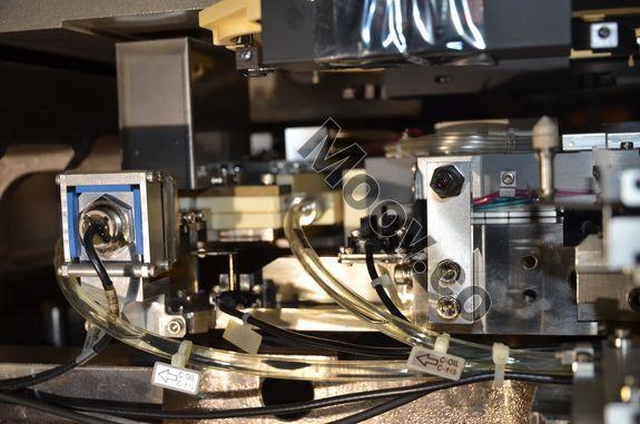
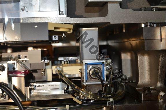
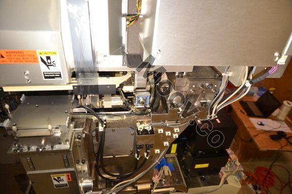
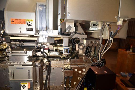
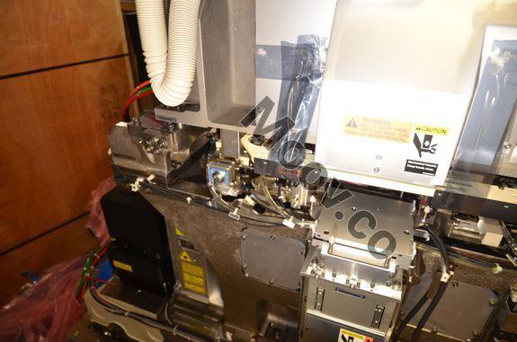
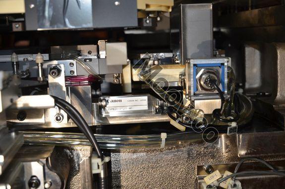
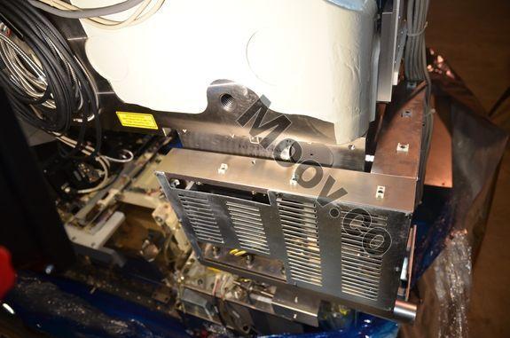
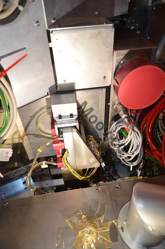
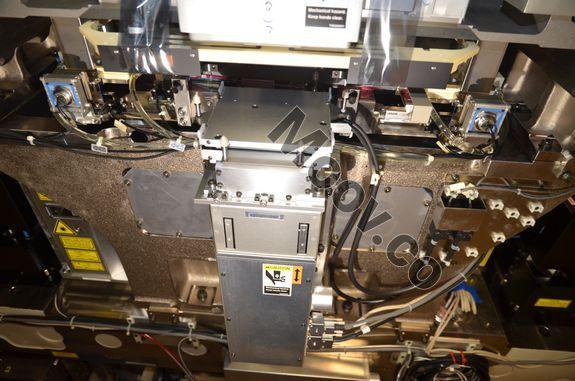
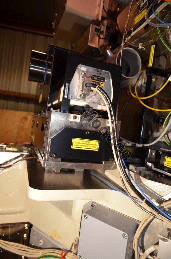
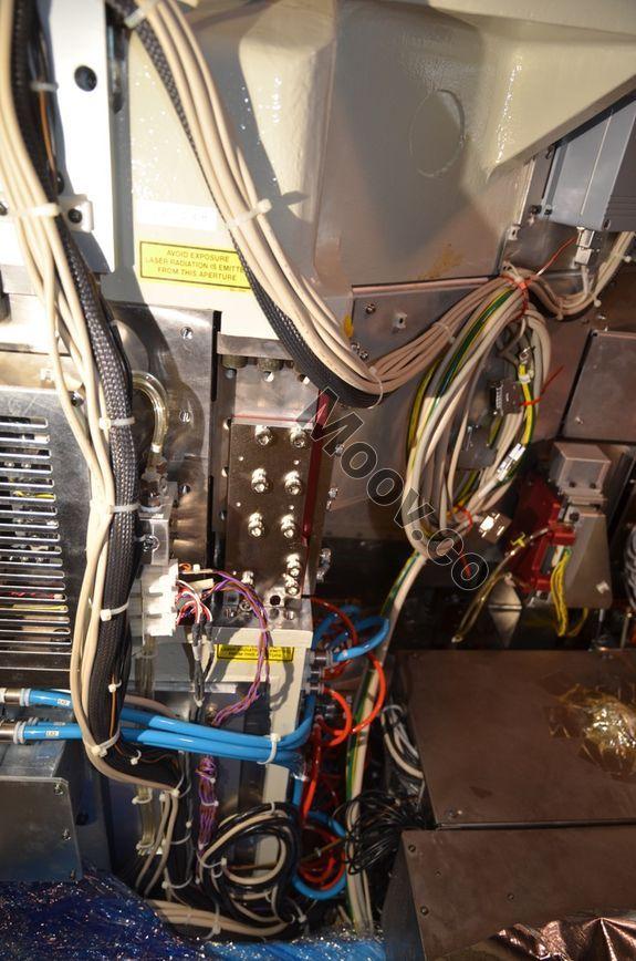
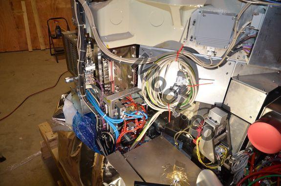
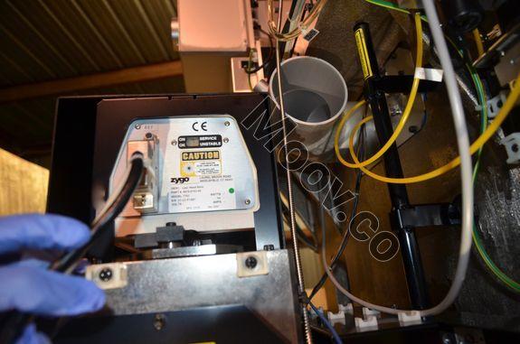
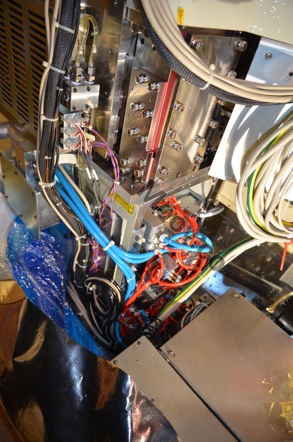
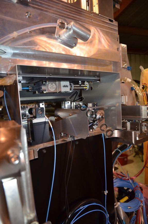
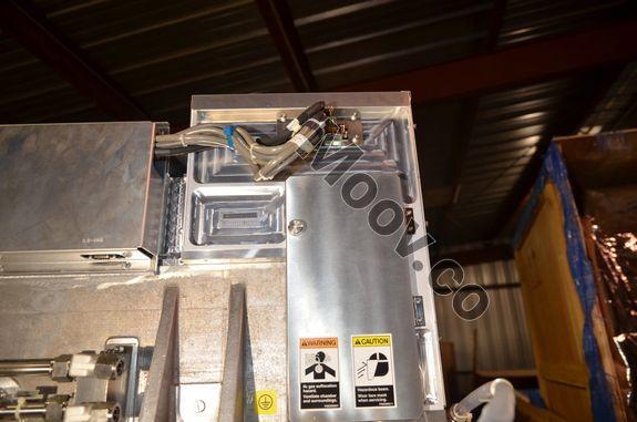
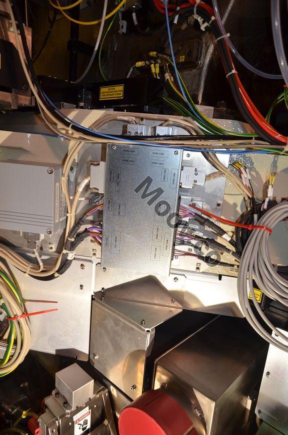
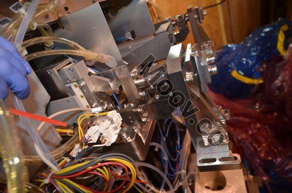
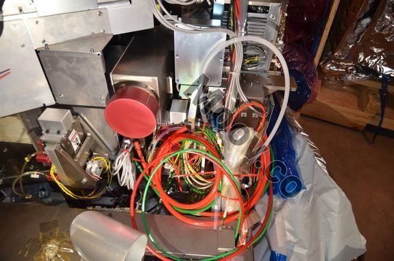
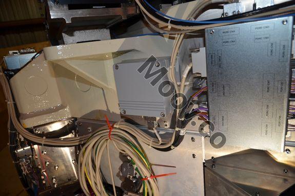
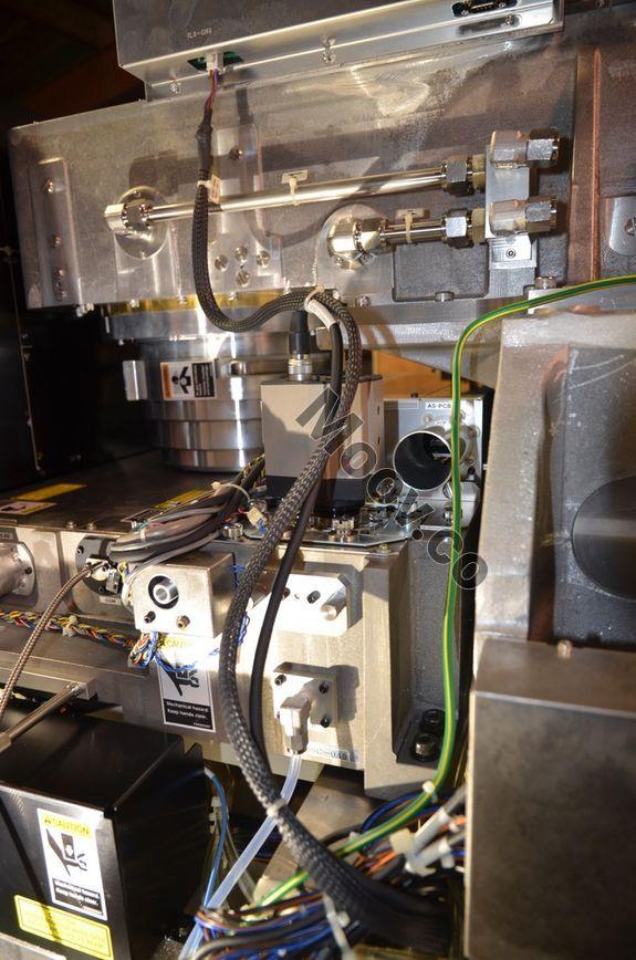
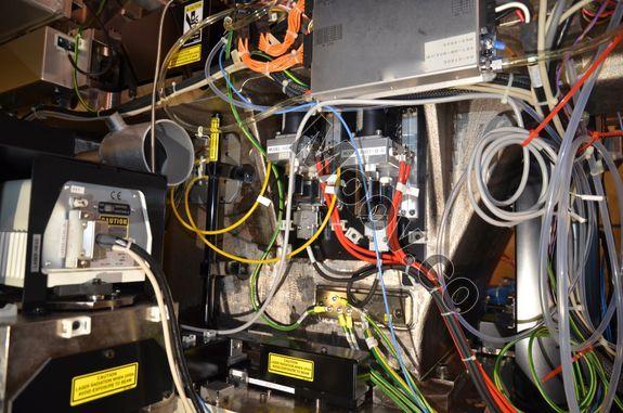
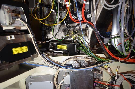
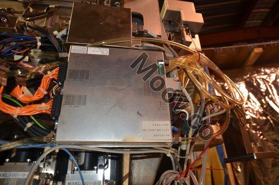
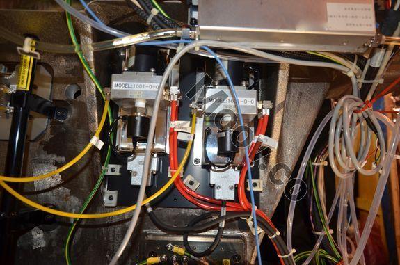
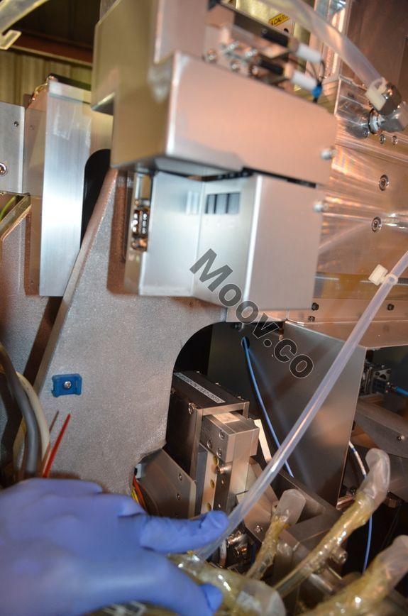
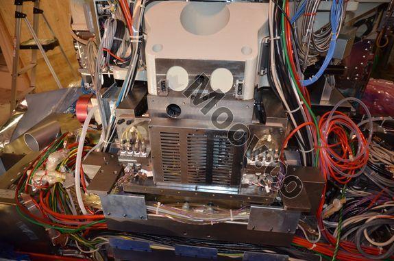
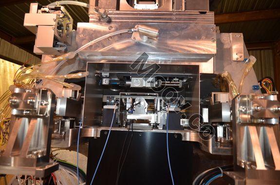
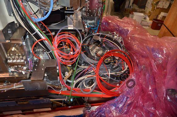
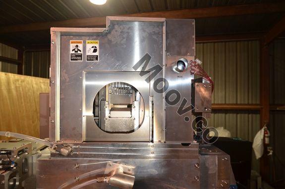
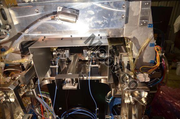
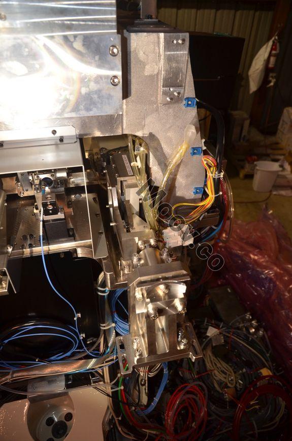
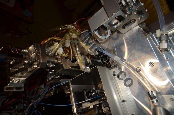
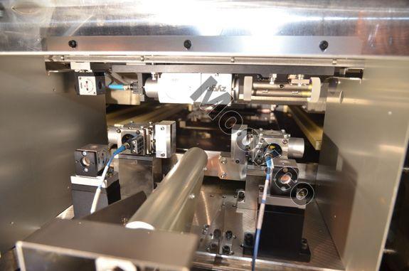
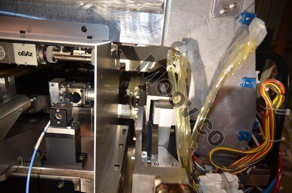
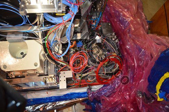
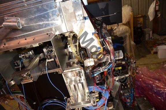
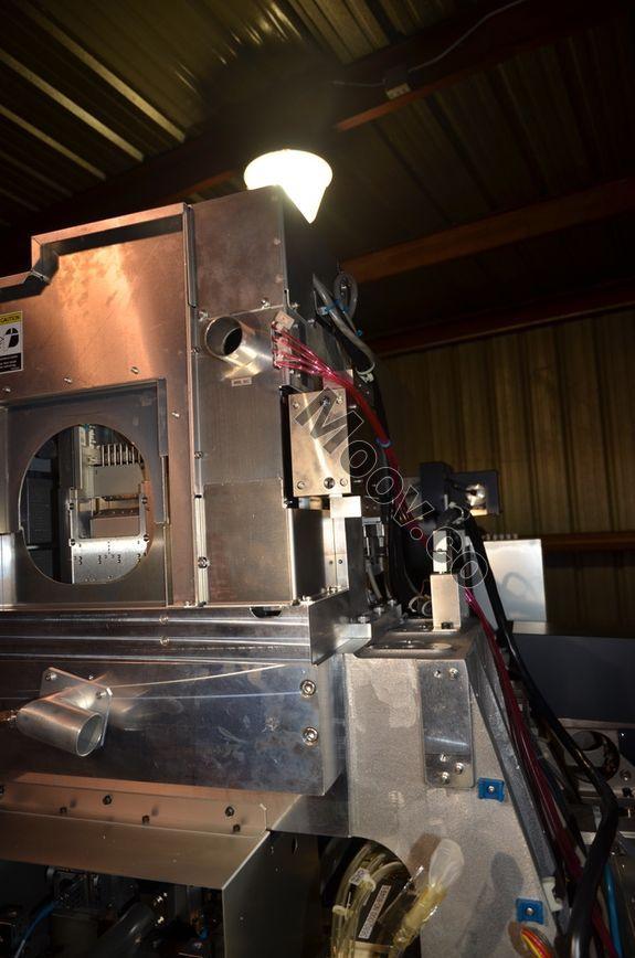
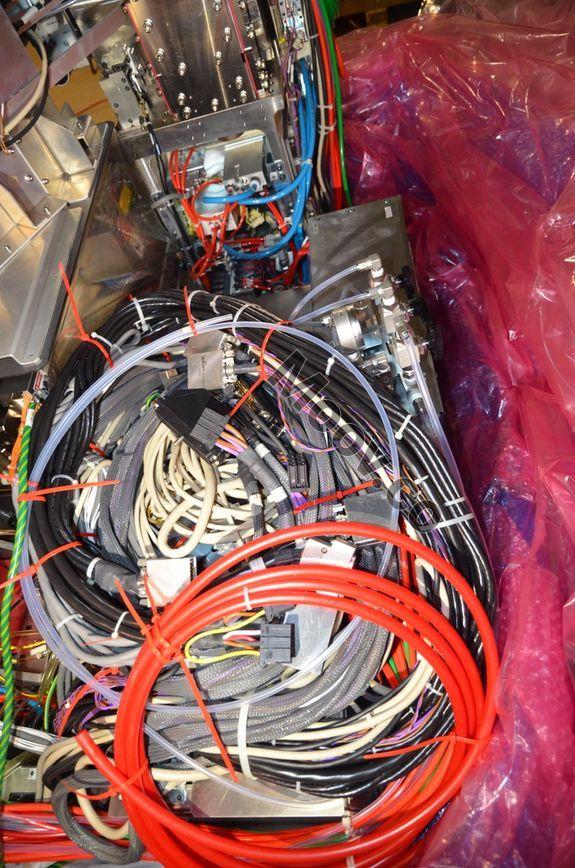
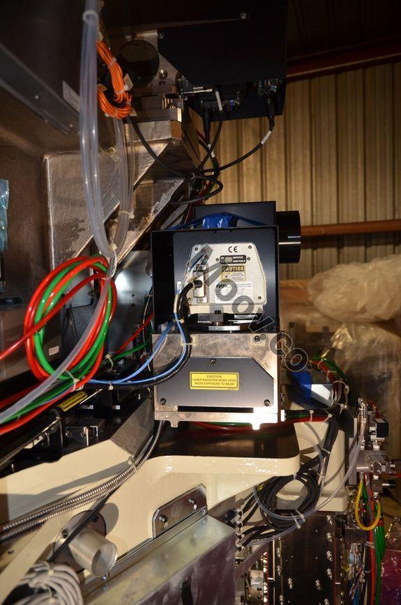
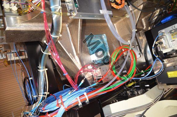
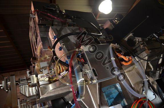
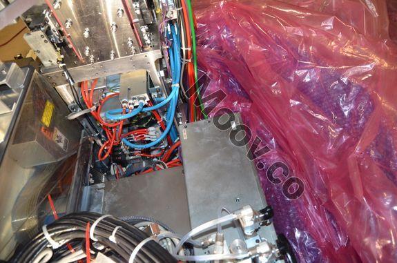
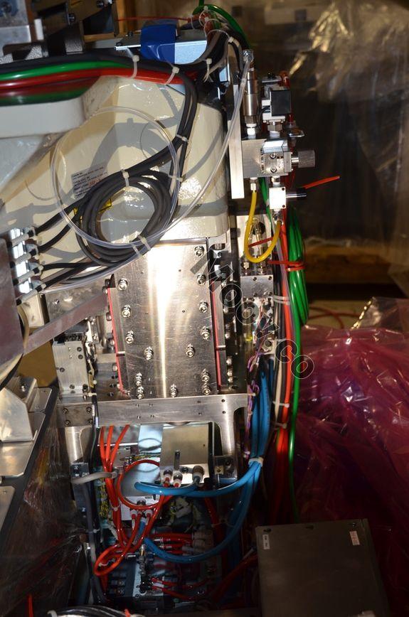
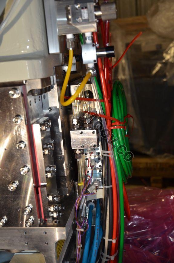
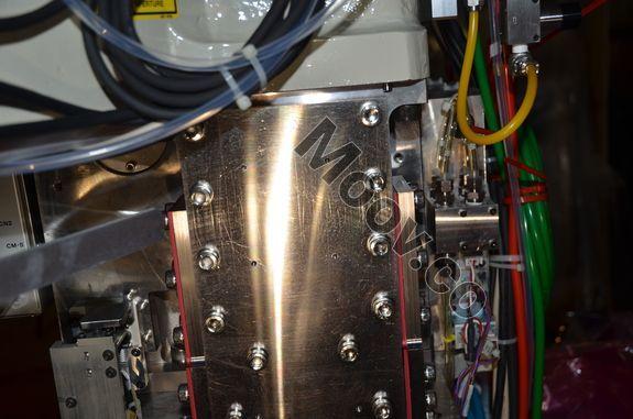
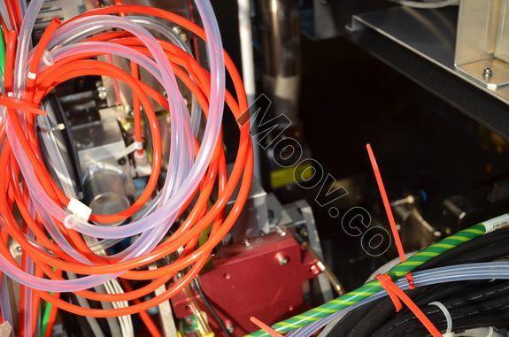
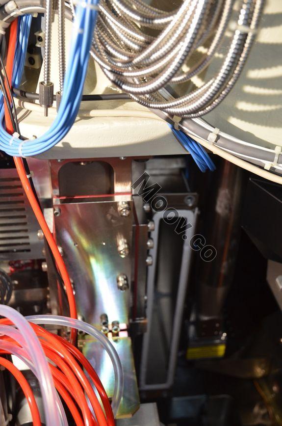
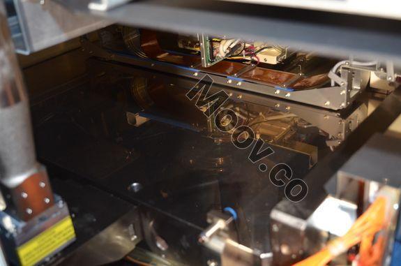
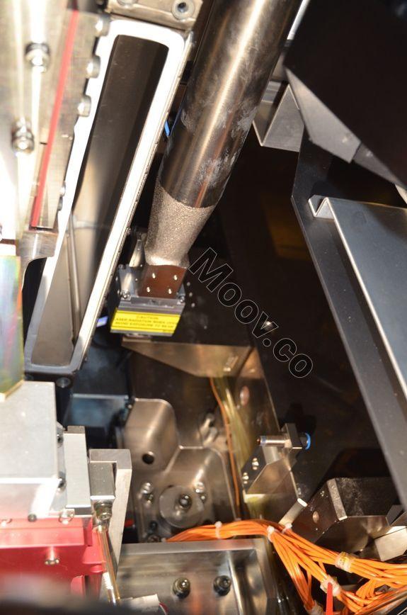
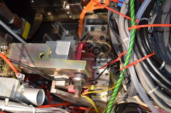
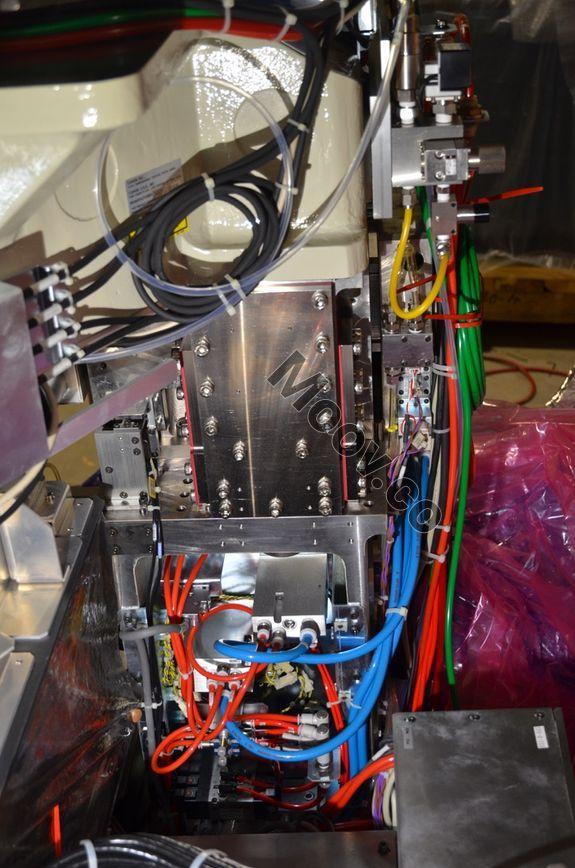
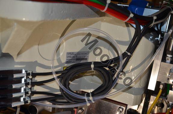
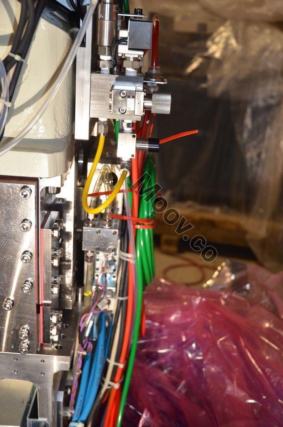
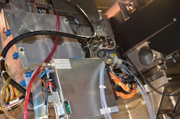
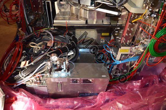
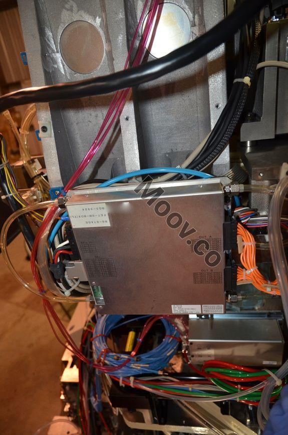
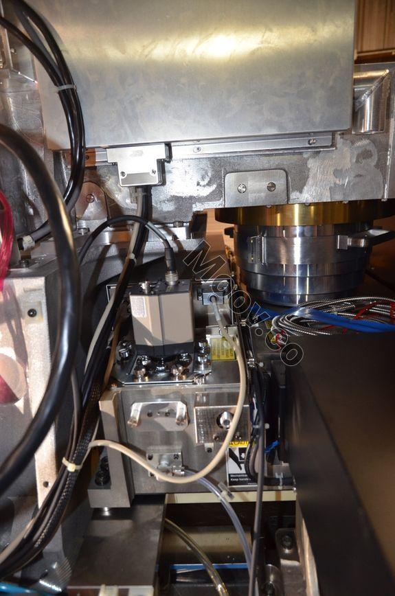
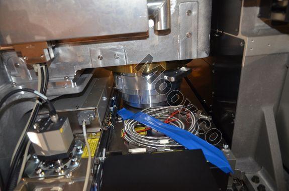
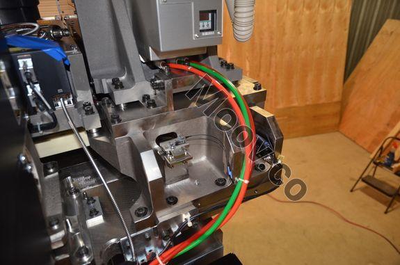
High NA covers 0.18 um to 0.15 um design rules using 248 KrF illumination. The wafer size can easily be changed between 200 mm and 300 mm with a simple conversion kit. The Platform features a reaction force receiver on both the reticle and wafer stages. Active dampers are added to the wafer stage to prevent machine vibrations from occuring via the fab floor. This allows much higher exposure speeds. The stage features frictionless air bearings and improved vibration isoltation. The wafer stage is of the new FLAT II design. The bar mirrors are hollow and the tilt plate is constructed with beams. This virtually eliminates mirror sag, and allows the stage weight for the 300 mm stage to remain about that of the previous models 200 mm stage. The lenses are assembled using Ultima PM1 data to minimise aberrations. Deinstalled, warehoused Alignment laser: Zygo Laser 6mm zygo p/n 8070-0102-05 Model 7702 Date March 2000 CE MARKED 12 SLOT RETICLE LIBRARY Robot type 6735A Power 200V 3 phase 2W, 1PE, 6.9 kva and 19.8 kva main unit weight 12260 kg *Scanner and environmental chamber) TCU 750 kg Laser and delivery optics 1557 kg Power box 100 kg Reduction ratio 4:1 Resolution 0.15 um illumination 248 nm (KrF) Image field size 26 mm x 33 mm reticle 6 inch square, 0.25 inch thickness Alignment - TTL off axis imaging and off axis imaging overlay accuracy better than 35 nm Through put better than 125 wph for 8 inch wafers Main body dimensions 230 cm w x 325 cm d x 280 cm height.OEM 모델 설명
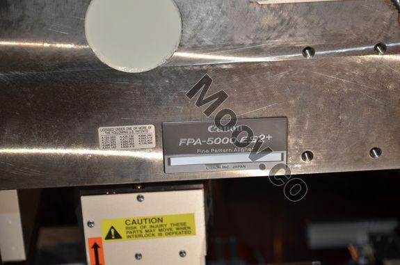
The FPA-5000ES2+ is a high-throughput 248-nanometer scanner for 0.15-micron ICs, introduced by Canon U.S.A. Inc.'s Semiconductor Equipment Division. It uses a 2-kilohertz, krypton-fluoride (KrF) excimer laser to expose 125 eight-inch wafers an hour and is aimed at a growing need for highly productive scanners with both 200- and 300-mm wafer capability. It has been designed to handle both 0.18- and 0.15-micron design rules, and allows field conversion from 200-mm to 300-mm wafer format within a day. It offers a 25% increase in throughput compared with its predecessor, the FPA-5000ES2.문서
문서 없음
CANON
FPA-5000ES2+

검증됨
카테고리
193 nm Step and Scan
주요 품목 세부 정보
조건:
Used
작동 상태:
알 수 없음
제품 ID:
29052
웨이퍼 사이즈:
알 수 없음
빈티지:
2000
Have Additional Questions?
Logistics Support
Available
Money Back Guarantee
Available
Transaction Insured by Moov
Available
Refurbishment Services
Available
CANON
FPA-5000ES2+
검증됨
카테고리
193 nm Step and Scan
마지막 검증일: 60일 이상 전

주요 품목 세부 정보
조건:
Used
작동 상태:
알 수 없음
제품 ID:
29052
웨이퍼 사이즈:
알 수 없음
빈티지:
2000
Logistics Support
Available
Money Back Guarantee
Available
Transaction Insured by Moov
Available
Refurbishment Services
Available
설명
설명 없음환경 설정
High NA covers 0.18 um to 0.15 um design rules using 248 KrF illumination. The wafer size can easily be changed between 200 mm and 300 mm with a simple conversion kit. The Platform features a reaction force receiver on both the reticle and wafer stages. Active dampers are added to the wafer stage to prevent machine vibrations from occuring via the fab floor. This allows much higher exposure speeds. The stage features frictionless air bearings and improved vibration isoltation. The wafer stage is of the new FLAT II design. The bar mirrors are hollow and the tilt plate is constructed with beams. This virtually eliminates mirror sag, and allows the stage weight for the 300 mm stage to remain about that of the previous models 200 mm stage. The lenses are assembled using Ultima PM1 data to minimise aberrations. Deinstalled, warehoused Alignment laser: Zygo Laser 6mm zygo p/n 8070-0102-05 Model 7702 Date March 2000 CE MARKED 12 SLOT RETICLE LIBRARY Robot type 6735A Power 200V 3 phase 2W, 1PE, 6.9 kva and 19.8 kva main unit weight 12260 kg *Scanner and environmental chamber) TCU 750 kg Laser and delivery optics 1557 kg Power box 100 kg Reduction ratio 4:1 Resolution 0.15 um illumination 248 nm (KrF) Image field size 26 mm x 33 mm reticle 6 inch square, 0.25 inch thickness Alignment - TTL off axis imaging and off axis imaging overlay accuracy better than 35 nm Through put better than 125 wph for 8 inch wafers Main body dimensions 230 cm w x 325 cm d x 280 cm height.OEM 모델 설명
The FPA-5000ES2+ is a high-throughput 248-nanometer scanner for 0.15-micron ICs, introduced by Canon U.S.A. Inc.'s Semiconductor Equipment Division. It uses a 2-kilohertz, krypton-fluoride (KrF) excimer laser to expose 125 eight-inch wafers an hour and is aimed at a growing need for highly productive scanners with both 200- and 300-mm wafer capability. It has been designed to handle both 0.18- and 0.15-micron design rules, and allows field conversion from 200-mm to 300-mm wafer format within a day. It offers a 25% increase in throughput compared with its predecessor, the FPA-5000ES2.문서
문서 없음