530
개요
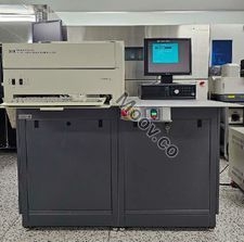
The SSM 530 is a fully automatic mapping system that provides a variety of electrical characterization measurements for non-patterned wafers used in epitaxial silicon production and front-end semiconductor processing. It has the same abilities as the SSM 5130, but it does not have a robot. The SSM 530 eliminates the need for costly metal and poly deposition processes by using a pneumatically controlled, non-damaging probe design and a top-side mercury contact. It features an extremely stable contact area and uses only a small quantity of mercury to make highly repeatable measurements for process development and process monitoring applications. Typical applications include EPI resistivity, low-k dielectric constant, and oxide integrity. The system can handle wafer diameters from 200 mm to 300 mm and can perform single-site and multiple-site maps. It also features automatic face-up loading to prevent wafer damage, precision pressure regulators for Hg contact, and PROCAP software that provides a full suite of measurements.
활성 등재물
2
서비스
검사, 보험, 감정, 물류