


설명
설명 없음환경 설정
환경 설정 없음OEM 모델 설명
Applied UVision® 3 system, the industry’s highest productivity DUV1 Brightfield wafer inspection tool with the critical-defect detection sensitivity required for 45 nanometer (nm) FEOL2 and immersion lithography. Delivering significant advancements to Applied’s breakthrough UVision technology, this next-generation system triples the number of laser beams scanning the wafer to provide 40% faster throughput than any competitive system. Two new imaging modes extend sensitivity to 20nm, and a new flexible automatic defect classification engine enables quick access to defects of interest and faster yield learning. imaging modes in the illumination and collection path which address the contrast versatility required for periphery areas; innovative algorithms of high defect accuracy and stitch-to-stitch detection enable enhanced sensitivity on edge of array and on high-end devices; dual screen configuration with High Resolution Review, which minimizes SEM review time; and new automatic classification capabilities provide quick access to defect-of-interest to reduce yield learning cycle. Additionally, UVision 3’s proprietary ActiveScan technique dynamically compensates for process and color variations within and across wafers.문서
문서 없음

카테고리
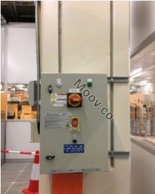
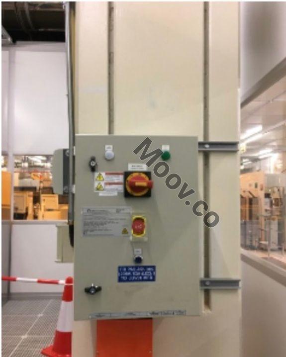
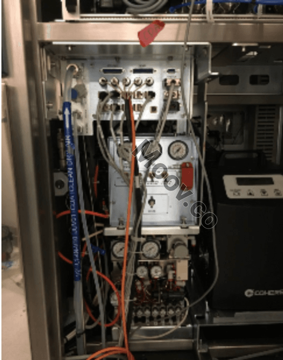
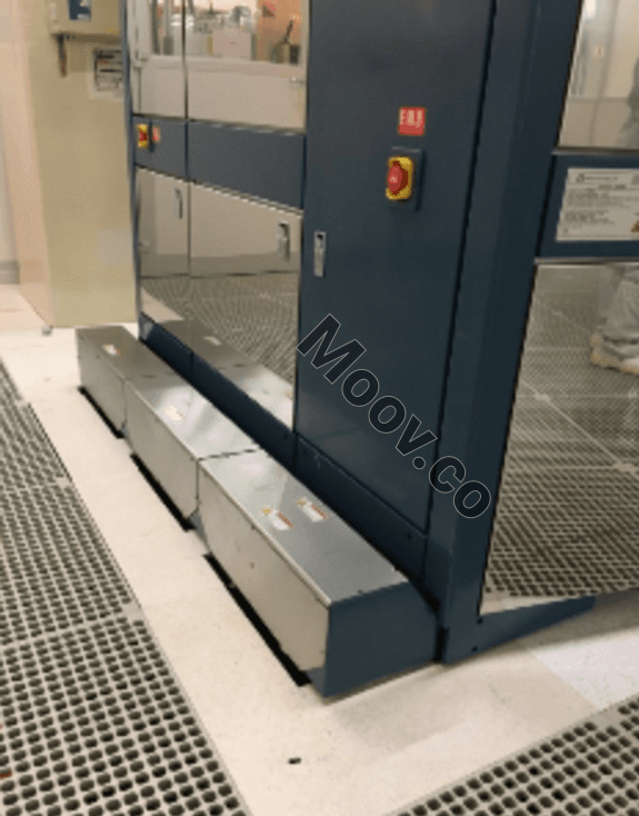
Defect Inspection
마지막 검증일: 60일 이상 전
주요 품목 세부 정보
조건:
Used
작동 상태:
알 수 없음
제품 ID:
29600
웨이퍼 사이즈:
알 수 없음
빈티지:
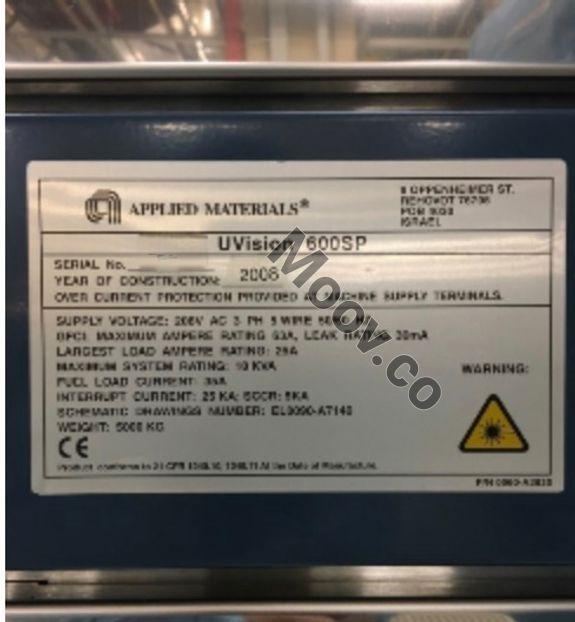
2008
Logistics Support
Available
Transaction Insured by Moov
Available
Refurbishment Services
Available
APPLIED MATERIALS (AMAT)
UVISION 3
카테고리
Defect Inspection
마지막 검증일: 60일 이상 전

주요 품목 세부 정보
조건:
Used
작동 상태:
알 수 없음
제품 ID:
29600
웨이퍼 사이즈:
알 수 없음
빈티지:
2008
Logistics Support
Available
Transaction Insured by Moov
Available
Refurbishment Services
Available
설명
설명 없음환경 설정
환경 설정 없음OEM 모델 설명
Applied UVision® 3 system, the industry’s highest productivity DUV1 Brightfield wafer inspection tool with the critical-defect detection sensitivity required for 45 nanometer (nm) FEOL2 and immersion lithography. Delivering significant advancements to Applied’s breakthrough UVision technology, this next-generation system triples the number of laser beams scanning the wafer to provide 40% faster throughput than any competitive system. Two new imaging modes extend sensitivity to 20nm, and a new flexible automatic defect classification engine enables quick access to defects of interest and faster yield learning. imaging modes in the illumination and collection path which address the contrast versatility required for periphery areas; innovative algorithms of high defect accuracy and stitch-to-stitch detection enable enhanced sensitivity on edge of array and on high-end devices; dual screen configuration with High Resolution Review, which minimizes SEM review time; and new automatic classification capabilities provide quick access to defect-of-interest to reduce yield learning cycle. Additionally, UVision 3’s proprietary ActiveScan technique dynamically compensates for process and color variations within and across wafers.문서
문서 없음