


설명
Operational upon removal from the fab. Skidded, vapor barrier bagged, wrapped. Not crated. Complete systems, with no missing parts.환경 설정
환경 설정 없음OEM 모델 설명
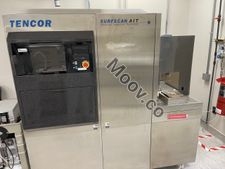
The AIT In-line Defect Inspection System is a high-throughput system that uses proprietary double-darkfield (DDF) laser scanning technology to detect defects, microscratches, and particulate contamination on wafers. It can inspect up to 30 wafers per hour at maximum sensitivity and has a low cost-per-inspection, making it economically feasible to perform in-line process monitoring at more process levels. The system achieves exceptional defect sensitivity through innovations such as a reduced laser spot size and a unique double-darkfield laser scattering design.문서
문서 없음

유사 등재물
모두 보기

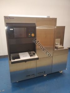

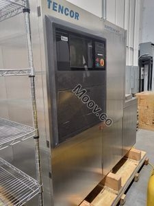


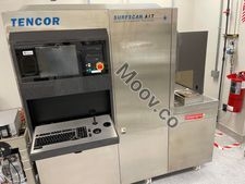
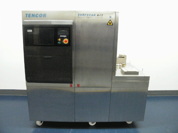


KLA
AIT I
카테고리
Defect Inspection
마지막 검증일: 60일 이상 전


주요 품목 세부 정보
조건:
Used
작동 상태:
알 수 없음
제품 ID:
131730
웨이퍼 사이즈:
알 수 없음
빈티지:
알 수 없음
Logistics Support
Available
Transaction Insured by Moov
Available
Refurbishment Services
Available
설명
Operational upon removal from the fab. Skidded, vapor barrier bagged, wrapped. Not crated. Complete systems, with no missing parts.환경 설정
환경 설정 없음OEM 모델 설명
The AIT In-line Defect Inspection System is a high-throughput system that uses proprietary double-darkfield (DDF) laser scanning technology to detect defects, microscratches, and particulate contamination on wafers. It can inspect up to 30 wafers per hour at maximum sensitivity and has a low cost-per-inspection, making it economically feasible to perform in-line process monitoring at more process levels. The system achieves exceptional defect sensitivity through innovations such as a reduced laser spot size and a unique double-darkfield laser scattering design.문서
문서 없음