AIT III
개요
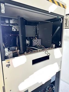
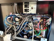
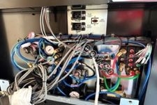
The AIT III is a high-throughput darkfield wafer inspection tool that can capture small defects resulting from the transition to 0.13 µm and smaller design rules. It has advanced noise suppression capabilities, making it suitable for films, CMP, photo, and etch applications. It is ideal for the development and ramp of 0.13 µm technology products and extends a fab’s current capability for production tool monitoring of yield-limiting defects. It offers improved capture of CMP and pattern transfer defects, superior suppression of grain, pattern noise and color variation, high defect signal-to-noise ratio with maximized surface selectivity, high throughput at required sensitivity, fast automated recipe setup, rigorous system-to-system matching, and is field upgradeable from the AIT II. It is also 300 mm capable with flexible automation options.
활성 등재물
11
서비스
검사, 보험, 감정, 물류