


설명
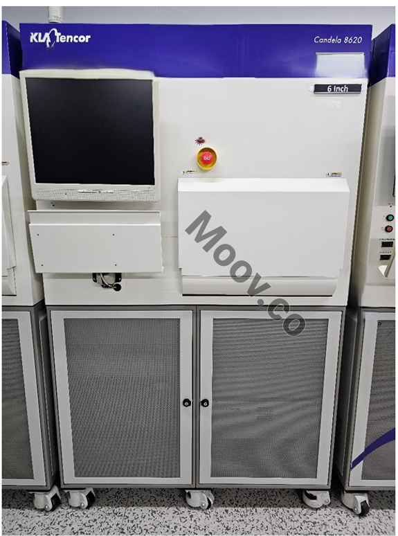
Wafer Size: 2 ~ 8 inch available (Currently 6" configured) Application S/W: 7.0 Build 11 OS Version: Windows XP professional SP3 Cassette Handling: Standard single puck with up to 200 mm cassette handler capability Illumination Source: Circumferential (50 mW, 405 nm), Radial (85 mW, 660 nm) Performance • Substrate Thickness: 380 ~ 1,300 µm • Defect Sensitivity: 0.08 µm (PSL on bare) Application Defect inspection of both opaque substrates such as Si, GaAs, and InP, as well as transparent materials such as SiC, GaN, sapphire, and glass. Utility • Physical Dimension (WDH): 110 * 138 * 180 cm • Weight Instrument: 860 lb (391 kg) • Input Power: 115 V 12 A 50/60 Hz • CDA: 95 ~ 110 PSI환경 설정
환경 설정 없음OEM 모델 설명
The Candela 8620 is an automated defect inspection system for LED substrates and epitaxy wafers. It provides enhanced quality control for materials such as gallium nitride, sapphire, and silicon carbide. Its proprietary optical design and detection technology can detect sub-micron defects that are not consistently identified by current inspection methods. This enables a production line monitor for yield-limiting defects, improving MOCVD reactor uptime and yield. The system can detect defects such as micro-scratches, micro-cracks, missing bumps, resist voids, hexagonal pits, and epi cracks, which can impact device performance, yield, and reliability.문서

카테고리
Defect Inspection
마지막 검증일: 60일 이상 전
주요 품목 세부 정보
조건:
Refurbished
작동 상태:
알 수 없음
제품 ID:
138243
웨이퍼 사이즈:
2"/50mm, 3"/75mm, 4"/100mm, 5"/125mm, 6"/150mm
빈티지:
2012
Logistics Support
Available
Transaction Insured by Moov
Available
Refurbishment Services
Available
유사 등재물
모두 보기


KLA
CANDELA 8620
카테고리
Defect Inspection
마지막 검증일: 60일 이상 전


주요 품목 세부 정보
조건:
Refurbished
작동 상태:
알 수 없음
제품 ID:
138243
웨이퍼 사이즈:
2"/50mm, 3"/75mm, 4"/100mm, 5"/125mm, 6"/150mm
빈티지:
2012
Logistics Support
Available
Transaction Insured by Moov
Available
Refurbishment Services
Available