


설명
설명 없음환경 설정
0.050 um Defect Sensitivity on Polished Bare Silicon Enhanced Rough Film Sensitivity Already upgraded with ENH SS laser Defect Map and Histogram with Zoom RTDC (Real Time Defect Classification) Map to Map Operator Interface Blower UnitOEM 모델 설명
The Surfscan SP1DLS is an unpatterned wafer inspection system that detects defects down to 50nm and provides complete defectivity and haze information in a single scan. It uses dual-laser illumination and has an optional Backside Inspection Module. It supports 200mm and 300mm wafer sizes and meets 300mm factory automation requirements.문서
문서 없음

유사 등재물
모두 보기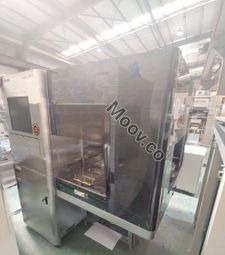


KLA
SP1 DLS
카테고리
Defect Inspection
마지막 검증일: 60일 이상 전


주요 품목 세부 정보
조건:
Used
작동 상태:
알 수 없음
제품 ID:
123843
웨이퍼 사이즈:
알 수 없음
빈티지:
2004
Logistics Support
Available
Transaction Insured by Moov
Available
Refurbishment Services
Available
설명
설명 없음환경 설정
0.050 um Defect Sensitivity on Polished Bare Silicon Enhanced Rough Film Sensitivity Already upgraded with ENH SS laser Defect Map and Histogram with Zoom RTDC (Real Time Defect Classification) Map to Map Operator Interface Blower UnitOEM 모델 설명
The Surfscan SP1DLS is an unpatterned wafer inspection system that detects defects down to 50nm and provides complete defectivity and haze information in a single scan. It uses dual-laser illumination and has an optional Backside Inspection Module. It supports 200mm and 300mm wafer sizes and meets 300mm factory automation requirements.문서
문서 없음