


설명
설명 없음환경 설정
IBA_HiCurOEM 모델 설명
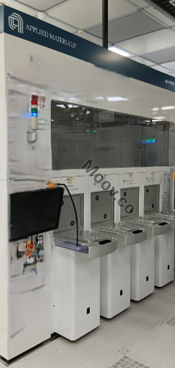
The Applied Quantum X Implant system, along with Applied's other technologies, meets the strict requirements for 65nm transistors. It offers high throughput at low energies, uniformity across all points and wafers, and precise motion control to prevent particle damage. The system is extendible to new applications for advanced logic and memory devices. Quantum X redefines fab productivity for high current ion implantation by providing single-wafer precision, ultra-low defect levels, and high throughput. Its innovative technology enables extendibility to high tilt implant and other new applications at 65nm and beyond. It features high throughput at low energies (200eV - 80keV) with all points, all wafers uniformity and two-dimensional parallel scanning with StepScan™ fixed beam technology for single wafer processing and up to 60° tilt angle문서
문서 없음

카테고리
High Current
마지막 검증일: 23일 전
주요 품목 세부 정보
조건:
Used
작동 상태:
알 수 없음
제품 ID:
144809
웨이퍼 사이즈:
12"/300mm
빈티지:
2006
Logistics Support
Available
Transaction Insured by Moov
Available
Refurbishment Services
Available


APPLIED MATERIALS (AMAT)
QUANTUM X
카테고리
High Current
마지막 검증일: 23일 전


주요 품목 세부 정보
조건:
Used
작동 상태:
알 수 없음
제품 ID:
144809
웨이퍼 사이즈:
12"/300mm
빈티지:
2006
Logistics Support
Available
Transaction Insured by Moov
Available
Refurbishment Services
Available
설명
설명 없음환경 설정
IBA_HiCurOEM 모델 설명
The Applied Quantum X Implant system, along with Applied's other technologies, meets the strict requirements for 65nm transistors. It offers high throughput at low energies, uniformity across all points and wafers, and precise motion control to prevent particle damage. The system is extendible to new applications for advanced logic and memory devices. Quantum X redefines fab productivity for high current ion implantation by providing single-wafer precision, ultra-low defect levels, and high throughput. Its innovative technology enables extendibility to high tilt implant and other new applications at 65nm and beyond. It features high throughput at low energies (200eV - 80keV) with all points, all wafers uniformity and two-dimensional parallel scanning with StepScan™ fixed beam technology for single wafer processing and up to 60° tilt angle문서
문서 없음