


설명
설명 없음환경 설정
환경 설정 없음OEM 모델 설명
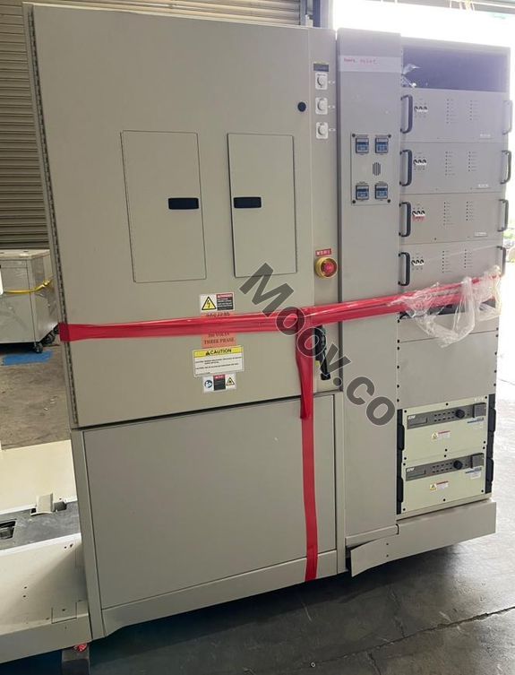
The VIISta PLAD is a multi-chamber tool built on a platform common with Varian Semiconductor’s VIISta family of implanters, the only truly complete platform available that covers all implant segments. The VIISta PLAD implants the entire wafer simultaneously by positioning the wafer directly in a chamber containing plasma of the desired species. A pulsed DC voltage applied to the wafer draws ions from the plasma at a precisely controlled energy, resulting in extremely fast high-dose implants. Pulsing the bias voltage allows the system to automatically neutralize any charge buildup on the wafer surface between pulses and measure the ion dose per pulse using a Faraday for closed-loop in-situ dose control. With throughput up to six times greater than beamline or modified-source beamline technologies, the VIISta PLAD has become an attractive solution for critical low-energy, high-dose applications, such as DRAM (dynamic random access memory) polysilicon gate doping.문서
문서 없음

카테고리
High Current
마지막 검증일: 60일 이상 전
주요 품목 세부 정보
조건:
Used
작동 상태:
알 수 없음
제품 ID:
137372
웨이퍼 사이즈:
12"/300mm
빈티지:
알 수 없음
Logistics Support
Available
Transaction Insured by Moov
Available
Refurbishment Services
Available


APPLIED MATERIALS (AMAT) / VARIAN
VIISta PLAD
카테고리
High Current
마지막 검증일: 60일 이상 전


주요 품목 세부 정보
조건:
Used
작동 상태:
알 수 없음
제품 ID:
137372
웨이퍼 사이즈:
12"/300mm
빈티지:
알 수 없음
Logistics Support
Available
Transaction Insured by Moov
Available
Refurbishment Services
Available
설명
설명 없음환경 설정
환경 설정 없음OEM 모델 설명
The VIISta PLAD is a multi-chamber tool built on a platform common with Varian Semiconductor’s VIISta family of implanters, the only truly complete platform available that covers all implant segments. The VIISta PLAD implants the entire wafer simultaneously by positioning the wafer directly in a chamber containing plasma of the desired species. A pulsed DC voltage applied to the wafer draws ions from the plasma at a precisely controlled energy, resulting in extremely fast high-dose implants. Pulsing the bias voltage allows the system to automatically neutralize any charge buildup on the wafer surface between pulses and measure the ion dose per pulse using a Faraday for closed-loop in-situ dose control. With throughput up to six times greater than beamline or modified-source beamline technologies, the VIISta PLAD has become an attractive solution for critical low-energy, high-dose applications, such as DRAM (dynamic random access memory) polysilicon gate doping.문서
문서 없음