


설명
Chamber door mounted interface for manipulators Broad beam plasma source ion column (Focus 250 µm) Manuals included Does not include manipulator.환경 설정
Vacuum system: EDWARDS XDS10 Scroll pump Sample stage: 5-Axes motorized X-Y-Z-rotate-tilt stage Step size: 100 nm (Minimum) High vacuum: 10^-10 mbar Travel: X, Y-Axis: 150 mm Z-Axis: 10 mm Tilt range: -5° to +60° Repeatability: 1 µm at 0° 2 µ at 52° Electron optics: Magnetic immersion lens Ultra-high brightness emitter Source: SCHOTTKY Field emitter Accelerating voltage: 350 V to 30 kV (Continously adjustable) Beam current: 1 pA - 22 nA Resolution: 0.9 nm at 15 kV 1.4 nm at 1 kV Ion optics: Sidewinder Field emission focused ion beam optics Liquid Gallium ion emitter Accelerating voltage: 0.5 kV to 30 kV (Continuously adjustable) Beam current: 1.5 pA - 20 nA Imaging resolution: 5 nm at 30 kV Milling resolution: 10 nn on Cr thin film Scanner: High-resolution digital scanning engine Resolution: 512x442, 1024x884, 2048x1768, 4096x3536 pixels Minimum dwell time: 25 ns/pixel Electronic scan rotation by 360° Patterning system: Maximum resolution: 64k x 64k Minimum dwell: 25 ns/pixel Maximum dwell: 25 ms/pixel Multiple pattern shapes Complex milling pattern through bitmap import Detectors: In-lens SE and BSE True Lens Detector (TLD) Everhart-Thornely SE Detector (ETD) 14-Segements solid state STEM II detector Chamber viewing IR CCD camera Controller: Microscope controller LCD Monitor, 19" Screen resolution: 1280x1024 Optical mouseOEM 모델 설명
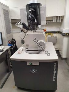
The Helios NanoLab 600 is a Dual Beam FIB/SEM (Focused Ion Beam/Scanning Electron Microscope) that is designed for high-end imaging during failure analysis. It features an extreme high-resolution column, a fine-probe ion source, and a 150 x 150 mm, five-axis, XY piezo stage. This makes it a smart investment for failure-analysis labs that require versatile sample handling, from packaged parts to eight-inch wafers. The Helios NanoLab 600 is particularly useful for cross-sectioning samples and delivers three-dimensional imaging, allowing you to quickly and efficiently locate and view device features from different angles. Additionally, patented beam chemistries can be used to highlight interface layers for imaging in the system, providing you with the most accurate data possible without additional preparation steps outside the system.문서

카테고리
SEM / FIB
마지막 검증일: 60일 이상 전
주요 품목 세부 정보
조건:
Used
작동 상태:
Installed / Running
제품 ID:
106194
웨이퍼 사이즈:
알 수 없음
빈티지:
알 수 없음
Logistics Support
Available
Transaction Insured by Moov
Available
Refurbishment Services
Available
유사 등재물
모두 보기


THERMOFISHER SCIENTIFIC / FEI / PHILIPS
HELIOS NANOLAB 600
카테고리
SEM / FIB
마지막 검증일: 60일 이상 전


주요 품목 세부 정보
조건:
Used
작동 상태:
Installed / Running
제품 ID:
106194
웨이퍼 사이즈:
알 수 없음
빈티지:
알 수 없음
Logistics Support
Available
Transaction Insured by Moov
Available
Refurbishment Services
Available