


설명
설명 없음환경 설정
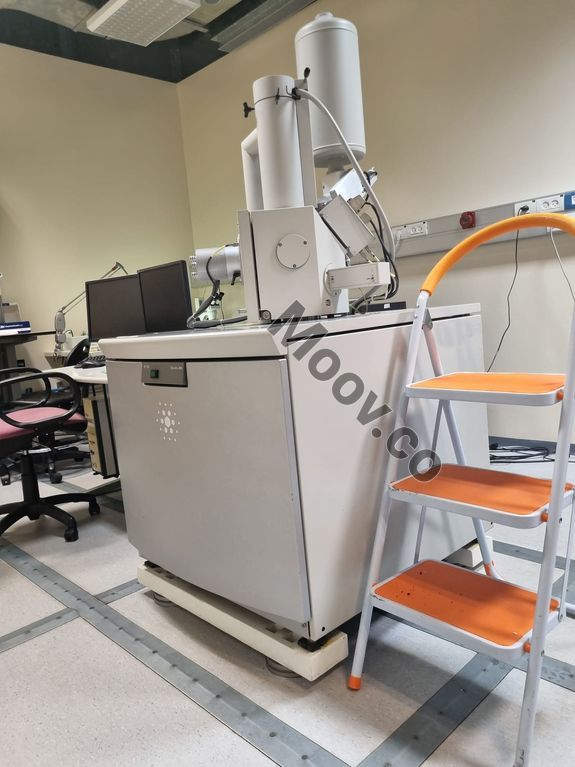
Electron optics • High-performance thermal emission- SEM column with dual-anode source emission geometry, fixed objective aperture and through-the-lens differential pumping • Filament lifetime > 100 hours Resolution - 3.0nm at 30kV (SE) - 4.0nm at 30kV (BSE) - 10nm at 3kV (SE) • Accelerating voltage: 200V – 30kV • Probe current: up to 2μA – continuously adjustable Detectors • Everhardt-Thornley SED • Low-vacuum SED (LFD) • Gaseous SED (GSED) • Solid-state BSED • Gaseous analytical BSED (GAD) Vacuum system • 1x 240 l/s TMP, 1x PVP • Patented through-the-lens differential pumping • Beam gas path length: 10 or 2 mm Chamber • 284mm left to right • 10mm analytical WD • 8 ports • EDX take-off angle: 35° 4-axis motorized stage • Eucentric goniometer stage • X,Y = 50mm • Z = 50mm (25mm motorized) • T = -15° to +75° (manual) • R = 360° continuous • Repeatability: 2μm System control • 32-bit graphical user interface with Windows XP, keyboard, optical mouse • Image display: 19-inch LCD, SVGA 1280 x 1024 • Single frame or 4-quadrant image display • 4-quadrant liveOEM 모델 설명
The Quanta 200 is a type of scanning electron microscope (SEM) that was once manufactured by FEI. This versatile instrument can be used in both high-vacuum and low-vacuum modes, allowing for the imaging of a wide range of samples. The electron beam in the Quanta 200 is produced by a traditional tungsten filament electron source, which can resolve features as small as 3 nm under ideal conditions. The instrument is equipped with standard Secondary Electron (SE) and Back Scatter Electron (BSE) detectors, as well as an Energy Dispersive X-ray Analysis (EDS) detector and an internal TV camera. Some of the Quanta 200’s features include SE, BSE, and EDS detectors; an accelerating voltage range of 200 V to 30 kV; a resolution of 3.0 nm at 30 kV; and a resolution of 10 nm at 3 kV.문서
문서 없음

카테고리
SEM / FIB
마지막 검증일: 4일 전
주요 품목 세부 정보
조건:
Used
작동 상태:
Deinstalled
제품 ID:
148416
웨이퍼 사이즈:
알 수 없음
빈티지:
알 수 없음
Logistics Support
Available
Transaction Insured by Moov
Available
Refurbishment Services
Available
유사 등재물
모두 보기


THERMOFISHER SCIENTIFIC / FEI / PHILIPS
QUANTA 200
카테고리
SEM / FIB
마지막 검증일: 4일 전


주요 품목 세부 정보
조건:
Used
작동 상태:
Deinstalled
제품 ID:
148416
웨이퍼 사이즈:
알 수 없음
빈티지:
알 수 없음
Logistics Support
Available
Transaction Insured by Moov
Available
Refurbishment Services
Available
설명
설명 없음환경 설정
Electron optics • High-performance thermal emission- SEM column with dual-anode source emission geometry, fixed objective aperture and through-the-lens differential pumping • Filament lifetime > 100 hours Resolution - 3.0nm at 30kV (SE) - 4.0nm at 30kV (BSE) - 10nm at 3kV (SE) • Accelerating voltage: 200V – 30kV • Probe current: up to 2μA – continuously adjustable Detectors • Everhardt-Thornley SED • Low-vacuum SED (LFD) • Gaseous SED (GSED) • Solid-state BSED • Gaseous analytical BSED (GAD) Vacuum system • 1x 240 l/s TMP, 1x PVP • Patented through-the-lens differential pumping • Beam gas path length: 10 or 2 mm Chamber • 284mm left to right • 10mm analytical WD • 8 ports • EDX take-off angle: 35° 4-axis motorized stage • Eucentric goniometer stage • X,Y = 50mm • Z = 50mm (25mm motorized) • T = -15° to +75° (manual) • R = 360° continuous • Repeatability: 2μm System control • 32-bit graphical user interface with Windows XP, keyboard, optical mouse • Image display: 19-inch LCD, SVGA 1280 x 1024 • Single frame or 4-quadrant image display • 4-quadrant liveOEM 모델 설명
The Quanta 200 is a type of scanning electron microscope (SEM) that was once manufactured by FEI. This versatile instrument can be used in both high-vacuum and low-vacuum modes, allowing for the imaging of a wide range of samples. The electron beam in the Quanta 200 is produced by a traditional tungsten filament electron source, which can resolve features as small as 3 nm under ideal conditions. The instrument is equipped with standard Secondary Electron (SE) and Back Scatter Electron (BSE) detectors, as well as an Energy Dispersive X-ray Analysis (EDS) detector and an internal TV camera. Some of the Quanta 200’s features include SE, BSE, and EDS detectors; an accelerating voltage range of 200 V to 30 kV; a resolution of 3.0 nm at 30 kV; and a resolution of 10 nm at 3 kV.문서
문서 없음