


설명
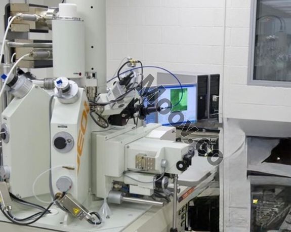
JEOL JXA-8530F Field Emission Electron Probe Microanalyzer (EPMA) with JEOL XEDS & xCLent Cathodoluminescence - This EPMA’s field emission electron gun produces a probe that is only 1/2 to 1/10 the size of that produced in a thermionic emission electron gun in a conventional EPMA, using a tungsten filament or a LaB6 tip. The FE electron gun is capable of producing a microprobe at low accelerating voltage even with high probe currents (10 to 100 nA), allowing for wavelength dispersive spectroscopy with high X-ray spatial resolution.환경 설정
- Detectable Elements: - WDS: (Be*) B to U - EDS: B to U - X-Ray Range: - WDS: 0.087 to 9.3 nm - EDS energy range: 20keV - Maximum Sample Size: 100mm x 100mm x 50mm (H) - Accelerating Voltage: 1 to 30 kV (0.1 kV steps) - Probe Current Range: 10-12 to 5x10⁻⁷ - Beam Current Stability: ± 0.3%/h - 3 nm (WD 11 mm, 30kV) - Minimum Probe Size: - 40nm (10kV, 1x10⁻⁸A) - 100nm (10kV, 1x10⁻⁷A) - Scanning Magnification: 40 to 300,000x (WD 11mm) - Scanning Image Resolution: Maximum 5120 x 3840OEM 모델 설명
Field Emission Electron Probe Microanalyzer문서
문서 없음


JEOL
JXA-8530F
카테고리
SEM / FIB
마지막 검증일: 4일 전


주요 품목 세부 정보
조건:
Used
작동 상태:
알 수 없음
제품 ID:
147931
웨이퍼 사이즈:
알 수 없음
빈티지:
알 수 없음
Logistics Support
Available
Transaction Insured by Moov
Available
Refurbishment Services
Available
설명
JEOL JXA-8530F Field Emission Electron Probe Microanalyzer (EPMA) with JEOL XEDS & xCLent Cathodoluminescence - This EPMA’s field emission electron gun produces a probe that is only 1/2 to 1/10 the size of that produced in a thermionic emission electron gun in a conventional EPMA, using a tungsten filament or a LaB6 tip. The FE electron gun is capable of producing a microprobe at low accelerating voltage even with high probe currents (10 to 100 nA), allowing for wavelength dispersive spectroscopy with high X-ray spatial resolution.환경 설정
- Detectable Elements: - WDS: (Be*) B to U - EDS: B to U - X-Ray Range: - WDS: 0.087 to 9.3 nm - EDS energy range: 20keV - Maximum Sample Size: 100mm x 100mm x 50mm (H) - Accelerating Voltage: 1 to 30 kV (0.1 kV steps) - Probe Current Range: 10-12 to 5x10⁻⁷ - Beam Current Stability: ± 0.3%/h - 3 nm (WD 11 mm, 30kV) - Minimum Probe Size: - 40nm (10kV, 1x10⁻⁸A) - 100nm (10kV, 1x10⁻⁷A) - Scanning Magnification: 40 to 300,000x (WD 11mm) - Scanning Image Resolution: Maximum 5120 x 3840OEM 모델 설명
Field Emission Electron Probe Microanalyzer문서
문서 없음