


설명
Waferbonder환경 설정
환경 설정 없음OEM 모델 설명
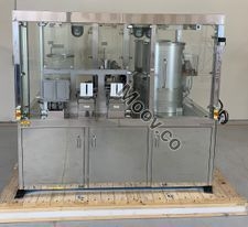
Automated production bonding system for a wide range of fusion/molecular wafer bonding applications SOI wafers are a promising new basic material for the microelectronics industry to produce faster and higher-performance microelectronic devices. Wafer bonding, as one key enabling technology for the SOI wafer fabrication process, achieves high-quality single-crystal silicon films on insulating substrates. With the EVG850 SOI production bonding system, all essential steps for SOI bonding – from cleaning and alignment to pre-bonding and IR-inspection – are combined. Thus, the EVG850 assures a high-yield production process for void-free SOI wafers up to 300 mm sizes. Being the only production system built to operate in high-throughput, high-yield environments, the EVG850 has been established as the industry standard in the SOI wafer market.문서
문서 없음

카테고리
Wafer Bonders
마지막 검증일: 60일 이상 전
주요 품목 세부 정보
조건:
Used
작동 상태:
알 수 없음
제품 ID:
41200
웨이퍼 사이즈:
8"/200mm
빈티지:
2012
Logistics Support
Available
Transaction Insured by Moov
Available
Refurbishment Services
Available
유사 등재물
모두 보기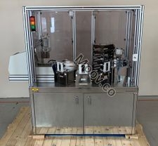


EVGroup (EVG)
EVG850
카테고리
Wafer Bonders
마지막 검증일: 60일 이상 전


주요 품목 세부 정보
조건:
Used
작동 상태:
알 수 없음
제품 ID:
41200
웨이퍼 사이즈:
8"/200mm
빈티지:
2012
Logistics Support
Available
Transaction Insured by Moov
Available
Refurbishment Services
Available
설명
Waferbonder환경 설정
환경 설정 없음OEM 모델 설명
Automated production bonding system for a wide range of fusion/molecular wafer bonding applications SOI wafers are a promising new basic material for the microelectronics industry to produce faster and higher-performance microelectronic devices. Wafer bonding, as one key enabling technology for the SOI wafer fabrication process, achieves high-quality single-crystal silicon films on insulating substrates. With the EVG850 SOI production bonding system, all essential steps for SOI bonding – from cleaning and alignment to pre-bonding and IR-inspection – are combined. Thus, the EVG850 assures a high-yield production process for void-free SOI wafers up to 300 mm sizes. Being the only production system built to operate in high-throughput, high-yield environments, the EVG850 has been established as the industry standard in the SOI wafer market.문서
문서 없음