




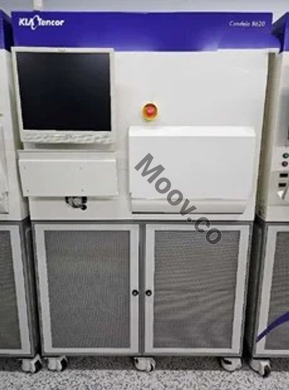
설명
설명 없음환경 설정
- Cassette Handling - Laser: Oblique(50mW, 405nm), Normal(85mW, 660nm) - Spot size: 5㎛ x 4㎛. - Handler: Mapping, Wafer centering on chuck and FFM: OK, Wafer loading/unloading: OK - Particle detection: smaller than 0.08㎛ on silicon substrate. - Scratch: 0.1㎛ wide, 1~2nm deep. - Pits and Bumps: 20㎛ diameter, 50Å; deep. - Stains: 20㎛ diameter, 10Å; thick. - can be used for both epi and bare substrate. - can be used for Si, GaAs, Al2O3,SiC substrate. - Substrate thickness: 350㎛ ~ 1,300㎛. - Air Balance system ULPA and HEPA air filter(replaced new one). - Input Power 115V 12A 50/60Hz - Input Air: CDA 90 PSI - Option: Cognex Wafer IDOEM 모델 설명
The Candela 8620 is an automated defect inspection system for LED substrates and epitaxy wafers. It provides enhanced quality control for materials such as gallium nitride, sapphire, and silicon carbide. Its proprietary optical design and detection technology can detect sub-micron defects that are not consistently identified by current inspection methods. This enables a production line monitor for yield-limiting defects, improving MOCVD reactor uptime and yield. The system can detect defects such as micro-scratches, micro-cracks, missing bumps, resist voids, hexagonal pits, and epi cracks, which can impact device performance, yield, and reliability.문서
문서 없음

카테고리
Defect Inspection
마지막 검증일: 9일 전
주요 품목 세부 정보
조건:
Refurbished
작동 상태:
알 수 없음
제품 ID:
153576
웨이퍼 사이즈:
8"/200mm
빈티지:
알 수 없음
Logistics Support
Available
Transaction Insured by Moov
Available
Refurbishment Services
Available
유사 등재물
모두 보기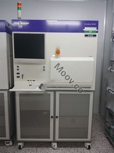



KLA
CANDELA 8620
카테고리
Defect Inspection
마지막 검증일: 9일 전


주요 품목 세부 정보
조건:
Refurbished
작동 상태:
알 수 없음
제품 ID:
153576
웨이퍼 사이즈:
8"/200mm
빈티지:
알 수 없음
Logistics Support
Available
Transaction Insured by Moov
Available
Refurbishment Services
Available
설명
설명 없음환경 설정
- Cassette Handling - Laser: Oblique(50mW, 405nm), Normal(85mW, 660nm) - Spot size: 5㎛ x 4㎛. - Handler: Mapping, Wafer centering on chuck and FFM: OK, Wafer loading/unloading: OK - Particle detection: smaller than 0.08㎛ on silicon substrate. - Scratch: 0.1㎛ wide, 1~2nm deep. - Pits and Bumps: 20㎛ diameter, 50Å; deep. - Stains: 20㎛ diameter, 10Å; thick. - can be used for both epi and bare substrate. - can be used for Si, GaAs, Al2O3,SiC substrate. - Substrate thickness: 350㎛ ~ 1,300㎛. - Air Balance system ULPA and HEPA air filter(replaced new one). - Input Power 115V 12A 50/60Hz - Input Air: CDA 90 PSI - Option: Cognex Wafer IDOEM 모델 설명
The Candela 8620 is an automated defect inspection system for LED substrates and epitaxy wafers. It provides enhanced quality control for materials such as gallium nitride, sapphire, and silicon carbide. Its proprietary optical design and detection technology can detect sub-micron defects that are not consistently identified by current inspection methods. This enables a production line monitor for yield-limiting defects, improving MOCVD reactor uptime and yield. The system can detect defects such as micro-scratches, micro-cracks, missing bumps, resist voids, hexagonal pits, and epi cracks, which can impact device performance, yield, and reliability.문서
문서 없음