


설명
설명 없음환경 설정
LAM Kiyo 45 Chamber Has missing partsOEM 모델 설명
The 2300 Versys Kiyo45 is a Reactive Ion Etch (RIE) system from Lam Research, part of the Kiyo Product Family. It is used to shape the electrically active materials of a semiconductor device with high precision and consistency. The Kiyo product family is known for its high-performance capabilities and productivity. The Versys Kiyo45 is used for various applications, including shallow trench isolation, source/drain engineering, high-k/metal gate, FinFET and tri-gate, and multi-patterning. It enables processing at sub-65 nm technology nodes.문서
문서 없음

카테고리
Dry / Plasma Etch
마지막 검증일: 60일 이상 전
주요 품목 세부 정보
조건:
Parts Tool
작동 상태:
Deinstalled
제품 ID:
97779
웨이퍼 사이즈:
알 수 없음
빈티지:
알 수 없음
Logistics Support
Available
Transaction Insured by Moov
Available
Refurbishment Services
Available
유사 등재물
모두 보기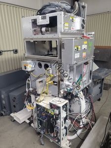


LAM RESEARCH CORPORATION
2300 VERSYS KIYO45
카테고리
Dry / Plasma Etch
마지막 검증일: 60일 이상 전


주요 품목 세부 정보
조건:
Parts Tool
작동 상태:
Deinstalled
제품 ID:
97779
웨이퍼 사이즈:
알 수 없음
빈티지:
알 수 없음
Logistics Support
Available
Transaction Insured by Moov
Available
Refurbishment Services
Available
설명
설명 없음환경 설정
LAM Kiyo 45 Chamber Has missing partsOEM 모델 설명
The 2300 Versys Kiyo45 is a Reactive Ion Etch (RIE) system from Lam Research, part of the Kiyo Product Family. It is used to shape the electrically active materials of a semiconductor device with high precision and consistency. The Kiyo product family is known for its high-performance capabilities and productivity. The Versys Kiyo45 is used for various applications, including shallow trench isolation, source/drain engineering, high-k/metal gate, FinFET and tri-gate, and multi-patterning. It enables processing at sub-65 nm technology nodes.문서
문서 없음