We value your privacy
We and our selected partners use cookies to enhance your browsing experience, serve personalized content, and analyze our traffic. By clicking "Accept All", you consent to our use of cookies. 더 알아보기


문서 없음
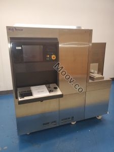
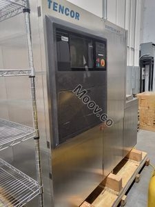
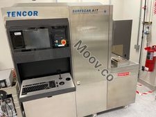
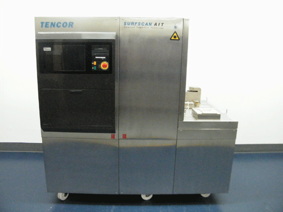
KLA
Used
알 수 없음
56599
알 수 없음
알 수 없음
문서 없음